ZHCSHN7B February 2018 – April 2018 TPSM84624
PRODUCTION DATA.
- 1 特性
- 2 应用
- 3 说明
- 4 修订历史记录
- 5 Pin Configuration and Functions
- 6 Specifications
-
7 Detailed Description
- 7.1 Overview
- 7.2 Functional Block Diagram
- 7.3
Feature Description
- 7.3.1 Adjusting the Output Voltage
- 7.3.2 Switching Frequency (RT)
- 7.3.3 Synchronization (CLK)
- 7.3.4 Output On/Off Enable (EN)
- 7.3.5 Input Capacitor Selection
- 7.3.6 Output Capacitor Selection
- 7.3.7 TurboTrans (TT)
- 7.3.8 Undervoltage Lockout (UVLO)
- 7.3.9 Soft Start (SS/TR)
- 7.3.10 Sequencing (SS/TR)
- 7.3.11 Power Good (PGOOD)
- 7.3.12 Safe Start-Up Into Pre-Biased Outputs
- 7.3.13 Overcurrent Protection
- 7.3.14 Thermal Shutdown
- 7.4 Device Functional Modes
- 8 Application and Implementation
- 9 Power Supply Recommendations
- 10Layout
- 11器件和文档支持
- 12机械、封装和可订购信息
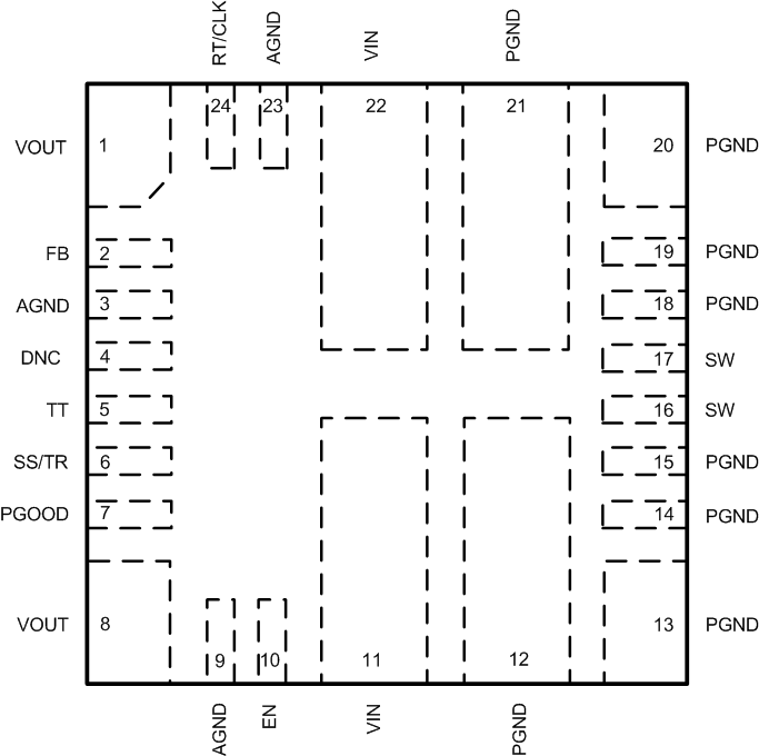
5 Pin Configuration and Functions
MOL Package
24-Pin QFM
Top View

Pin Functions
| PIN | TYPE(1) | DESCRIPTION | |
|---|---|---|---|
| NAME | NO. | ||
| AGND | 3, 9, 23 | G | Analog ground. Zero voltage reference for internal references and logic. These pins should be connected to one another externally using an analog ground plane on the PCB. Do not connect this pin to PGND; the connection is made internal to the device. |
| DNC | 4 | Do Not Connect. Do not connect this pin to AGND, PGND, or to any other voltage. This pin is connected to internal circuitry. | |
| EN | 10 | I | Enable. Float or pull high to enable the device. Connect a resistor divider to this pin to implement adjustable undervoltage lockout and hysteresis. |
| FB | 2 | I | Feedback input of the regulator. Connect the output voltage feedback resistor divider to this pin. |
| PGND | 12, 13, 14, 15, 18, 19, 20, 21 | G | Power ground. This is the return current path for the power stage of the device. Connect these pins to the input source, the load, and to the bypass capacitors associated with VIN and VOUT using power ground planes on the PCB. Pads 12 and 21 should be connected to the ground planes using multiple vias for improved thermal performance. |
| PGOOD | 7 | O | Power-Good flag. This open drain output asserts low if the output voltage is outside of the PGOOD thresholds, VIN is lower than its UVLO threshold, EN is low, device is in thermal shutdown or device is in soft-start. Use a 10-kΩ to 100-kΩ pullup resistor to logic rail or other DC voltage no higher than 6.5 V. |
| RT/CLK | 24 | I | Switching frequency setting pin. In RT mode, an external timing resistor adjusts the switching frequency. In CLK mode, the device synchronizes to an external clock input to this pin. |
| SS/TR | 6 | I | Soft-start and tracking pin. Connecting an external capacitor to this pin adjusts the output voltage soft-start ramp slower than its 1.25-ms default setting. A voltage applied to this pin allows for tracking and sequencing control. |
| SW | 16, 17 | O | Switch node. Do not place any external components on these pins or tie them to a pin of another function. |
| TT | 5 | I | TurboTrans pin. Internal loop compensation network. Connect the required TurboTrans resistor between this pin and AGND. See the TurboTrans (TT) section for the value of the resistor. Do not leave this pin floating. |
| VIN | 11, 22 | I | Input voltage. Supplies voltage to the power switches of the converter and all of the internal circuitry. Connect these pins to the input source and connect external input capacitors between these pins and PGND, close to the device. These pins should be connected to internal VIN layers using multiple vias for improved thermal performance. |
| VOUT | 1, 8 | O | Output voltage. These pins are connected to the internal output inductor. Connect these pins to the output load and connect external output capacitors between these pins and PGND, close to the device, and connect these pins to internal VOUT layers using multiple vias for improved thermal performance. |
(1) G = Ground, I = Input, O = Output