ZHCSHH6B January 2018 – JANUARY 2019 TPSM846C24
PRODUCTION DATA.
- 1 特性
- 2 应用
- 3 说明
- 4 修订历史记录
- 5 Pin Configuration and Functions
- 6 Specifications
-
7 Detailed Description
- 7.1 Overview
- 7.2 Functional Block Diagram
- 7.3
Feature Description
- 7.3.1 Minimum Capacitance Requirements
- 7.3.2 Setting the Compensation Network
- 7.3.3 Transient Response
- 7.3.4 Setting the Output Voltage
- 7.3.5 Differential Remote Sense
- 7.3.6 Switching Frequency and Synchronization
- 7.3.7 Prebiased Output Start-Up
- 7.3.8 Power-Good (PGOOD) Indicator
- 7.3.9 Linear Regulators BP3 and BP6
- 7.3.10 Parallel Application
- 7.3.11 Parallel Operation
- 7.3.12 Overtemperature Protection
- 7.3.13 Overcurrent Protection
- 7.3.14 Output Overvoltage and Undervoltage Protection
- 7.4 Device Functional Modes
- 8 Application and Implementation
- 9 Power Supply Recommendations
- 10Layout
- 11器件和文档支持
- 12机械、封装和可订购信息
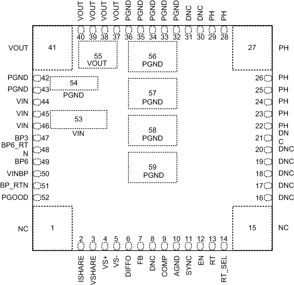
5 Pin Configuration and Functions
MOL Package
59-Pin BQFN
Top View

Pin Functions
| PIN | I/O | DESCRIPTION | |
|---|---|---|---|
| NAME | NO. | ||
| AGND | 10 | G | Analog ground for the controller circuitry. This pin is internally connected to PGND. |
| BP_RTN | 51 | G | Return path for VINBP and BP3. This pin is internally connected to PGND, pad 59. |
| BP3 | 47 | O | Output of the internal 3.3-V regulator. Bypass this pin with a minimum of 2.2-µF to BP_RTN. Can be used as a pullup termination voltage for PGOOD and EN signals. |
| BP6 | 49 | O | Output of the internal 6.5-V regulator that powers the driver stage of the device. Bypass this pin with a minimum of 2.2 µF to BP6_RTN. |
| BP6_RTN | 48 | G | Power ground return path for BP6 bypass cap. |
| COMP | 9 | O | Output of the error amplifier. |
| DIFFO | 6 | O | Output of the remote sense differential amplifier. This provides remote sensing for output voltage reporting and the voltage control loop. |
| DNC | 8, 16, 17, 18,
19, 20, 21, 30, 31 |
– | Do Not Connect. Do not connect these pins to AGND, PGND to a different DNC pin or to any other voltage. These pins are connected to internal circuitry. Each pin must be soldered to an isolated pad. |
| EN | 12 | I | EN pin. To enable, pull this pin up to a voltage less than 5.5 V using a 10-kΩ resistor. Pull this pin to AGND to disable the device. |
| FB | 7 | I | Feedback pin for the control loop. |
| ISHARE | 2 | I | Current sharing signal for parallel operation. |
| NC | 1, 15 | – | Not Connected. These pins are internally isolated from any signal and all other pins. Each pin must be soldered to a pad on the PCB. These pins can be left isolated, or connected to AGND or PGND. |
| PGND | 32, 33, 34, 35
36, 42, 43, 54 56, 57, 58, 59 |
G | Power ground of the device. This is the return current path for the power stage of the device. Connect these pins to the bypass capacitors associated with VIN and VOUT. Connect pads 56, 57, 58, and 59 to the PCB ground planes using multiple vias for optimal thermal performance. All pins must be connected together externally with a copper plane or pour directly under the device. |
| PGOOD | 52 | O | Power-good indicator. This pin is an open-drain output, which asserts low during any fault conditions. Requires a pullup resistor. |
| PH | 22, 23, 24, 25
26, 27, 28, 29 |
O | Phase switch node. Do not connect any external components to these pins or tie them to a pin of a different function. |
| RT | 13 | I | Frequency-setting resistor. To operate the device at its default switching frequency, make no connection to this pin. To operate at a different switching frequency, connect a resistor from this pin to AGND. |
| RT_SEL | 14 | I | RT resistor select. To operate the device at its default switching frequency, connect this pin to AGND. To operate at a different switching frequency, let this pin float. |
| SYNC | 11 | I/O | Frequency synchronization pin. In a stand-alone application or as the Master device in a parallel configuration, the SYNC pin is configured as a SYNC-IN pin and power conversion is synchronized to the rising edge of a 50% duty cycle external clock applied to this pin.
For a slave device in a parallel configuration, power conversion is synchronized to the falling edge of the incoming clock. |
| VIN | 44, 45, 46, 53 | I | Input switching voltage pins. These pins supply voltage to the power switches of the converter. |
| VINBP | 50 | I | Input power to the controller circuitry. Bypass this pin with a minimum of 1-µF to BP_RTN. This pin is internally connected to VIN. |
| VOUT | 37, 38, 39,
40, 41, 55 |
O | Output voltage. These pins are connected to the internal output inductor. Connect these pins to the output load and connect external bypass capacitors between these pins and PGND. |
| VS+ | 4 | I | Positive input of the remote sense amplifier. Connect this pin to VOUT at the load for best voltage regulation. Do not let this pin float. |
| VS– | 5 | I | Negative input of the remote sense amplifier. Connect this pin to ground at the load for best voltage regulation. Do not let this pin float. |
| VSHARE | 3 | I/O | Voltage sharing signal for parallel operation. |