ZHCSFS5 December 2016 TPSM84A21
PRODUCTION DATA.
- 1 降压稳压器
- 2 应用
- 3 说明
- 4 修订历史记录
- 5 Pin Configuration and Functions
- 6 Specifications
-
7 Detailed Description
- 7.1 Overview
- 7.2 Functional Block Diagram
- 7.3
Feature Description
- 7.3.1 Adjusting the Output Voltage (VADJ)
- 7.3.2 Input and Output Capacitance
- 7.3.3 Transient Response
- 7.3.4 Oscillator Frequency
- 7.3.5 External Clock Syncronization
- 7.3.6 Soft Start
- 7.3.7 Power Good (PGOOD)
- 7.3.8 Gate Driver (VG)
- 7.3.9 Startup into Pre-biased Outputs
- 7.3.10 Thermal Shutdown
- 7.3.11 Overcurrent Protection
- 7.3.12 Output Undervoltage/Overvoltage Protection
- 7.3.13 Enable (EN)
- 7.3.14 Undervoltage Lockout (UVLO)
- 7.4 Device Functional Modes
- 8 Application and Implementation
- 9 Power Supply Recommendations
- 10Layout
- 11器件和文档支持
- 12机械、封装和可订购信息
10 Layout
10.1 Layout Guidelines
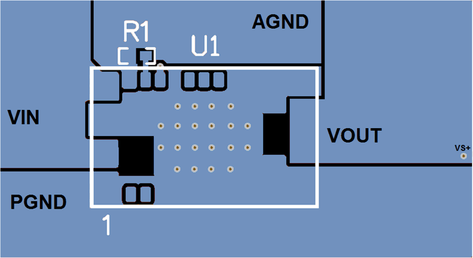
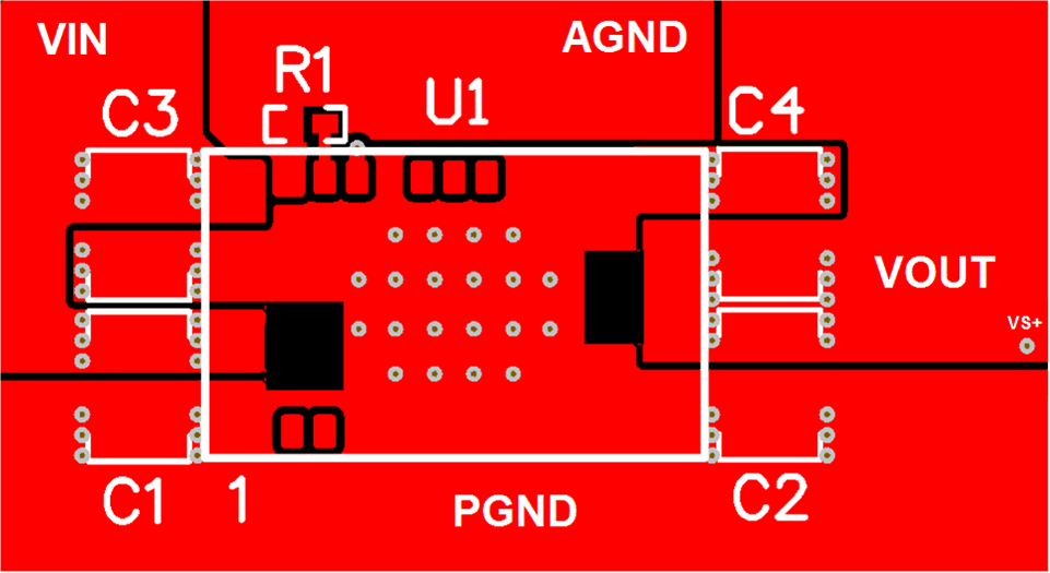
To achieve optimal electrical and thermal performance, an optimized PCB layout is required. Figure 20 and Figure 22 show typical, top-side PCB layouts. Some considerations for an optimized layout are:
- Use large copper areas for power planes (VIN, VOUT, and PGND) to minimize conduction loss and thermal stress.
- When adding input and output ceramic capacitors, place them close to the device pins to minimize high frequency noise.
- Locate any additional output capacitors between the ceramic capacitors and the load.
- Keep AGND and PGND separate from one another. The connection is made internal to the device.
- Place RSET as close as possible to the VADJ pin.
- Use multiple vias to connect the power planes to internal layers.
10.2 Layout Examples
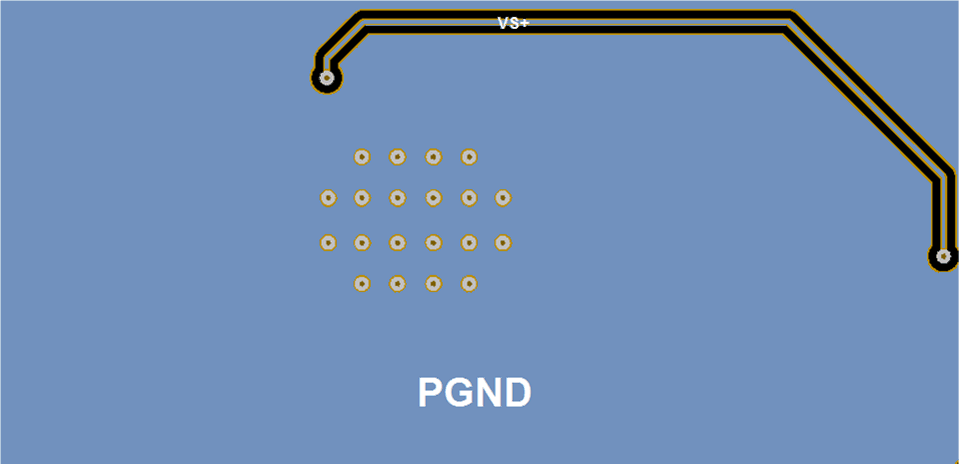
The layout shown in Figure 20 shows the minimum solution size with only a single voltage setting resistor (R1) as the only additional required component. Figure 21 shows a typical internal PCB layer with a trace connecting the VS+ pin to VOUT near the load.
 Figure 20. Minimum Component Layout
 Figure 21. VS+ Trace on Internal Layer
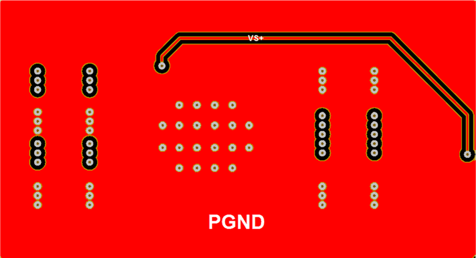
Figure 22 shows a layout with the placement of additional ceramic input capacitors (C1, C3) and ceramic output capacitors (C2, C4) for designs that require additional ripple reduction or improved transient response. Figure 23 shows a typical internal PCB layer with a trace connecting the VS+ pin to VOUT near the load
 Figure 22. Layout with Optional CIN and COUT
 Figure 23. VS+ Trace on Internal Layer