ZHCSFS5 December 2016 TPSM84A21
PRODUCTION DATA.
- 1 降压稳压器
- 2 应用
- 3 说明
- 4 修订历史记录
- 5 Pin Configuration and Functions
- 6 Specifications
-
7 Detailed Description
- 7.1 Overview
- 7.2 Functional Block Diagram
- 7.3
Feature Description
- 7.3.1 Adjusting the Output Voltage (VADJ)
- 7.3.2 Input and Output Capacitance
- 7.3.3 Transient Response
- 7.3.4 Oscillator Frequency
- 7.3.5 External Clock Syncronization
- 7.3.6 Soft Start
- 7.3.7 Power Good (PGOOD)
- 7.3.8 Gate Driver (VG)
- 7.3.9 Startup into Pre-biased Outputs
- 7.3.10 Thermal Shutdown
- 7.3.11 Overcurrent Protection
- 7.3.12 Output Undervoltage/Overvoltage Protection
- 7.3.13 Enable (EN)
- 7.3.14 Undervoltage Lockout (UVLO)
- 7.4 Device Functional Modes
- 8 Application and Implementation
- 9 Power Supply Recommendations
- 10Layout
- 11器件和文档支持
- 12机械、封装和可订购信息
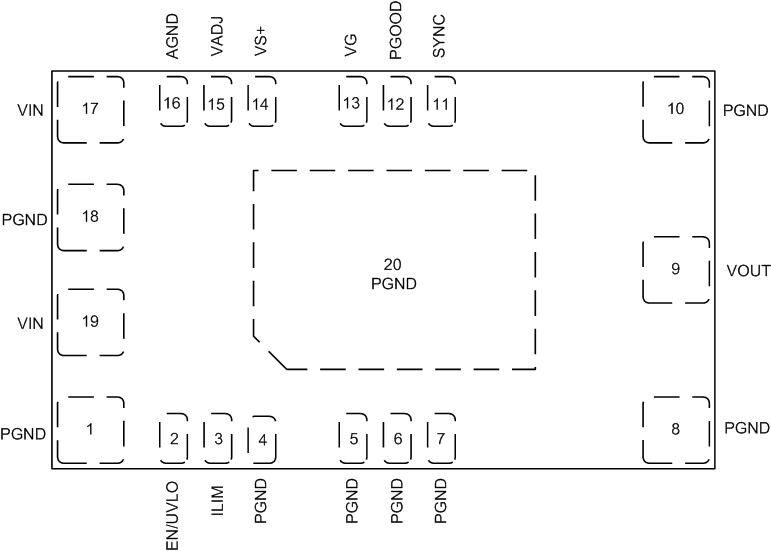
5 Pin Configuration and Functions
MOJ Package
20-Pin QFM
Top View

Pin Functions
| PIN | I/O | DESCRIPTION | |
|---|---|---|---|
| NAME | NO. | ||
| AGND | 16 | — | Zero voltage reference for analog control circuitry. Connect RSET between this pin and VADJ close to the device. Do not connect this pin to PGND; the connection is made internal to the device. |
| EN/UVLO | 2 | I | Enable and UVLO adjust pin. When this pin voltage is low, the device is disabled. Use an open drain, open collector, or a suitable logic gate device to control the enable function. A resistor divider between this pin, PGND, and VIN adjusts the UVLO voltage. |
| ILIM | 3 | I | Current limit setting pin. Leave this open for the full current limit threshold of 15 A. Connect a 47 kΩ resistor between this pin and PGND to reduce the current limit threshold to 11.25 A. |
| PGND | 1, 4, 5, 6, 7, 8, 10, 18, 20 | — | Power ground of the device. Connect these pins to the power ground plane of the PCB. Thermal vias to internal ground planes should be added beneath pin 20. |
| PGOOD | 12 | O | Power good indicator. This pin is an open-drain output and will assert low if the output voltage is greater than ±5% from the programmed value or due to thermal shutdown, under-voltage, or EN shutdown. A pull-up resistor is required. VG can be used as a PGOOD pull-up source. |
| VS+ | 14 | I | Remote sense connection. This pin must be connected to VOUT at the load or at the device pins. Connect the pin to VOUT at the load for improved regulation. |
| SYNC | 11 | I | External clock synchronization pin. An external clock signal can be applied to this pin to synchronize the switching frequency within ±10% of the nominal switching frequency (4 MHz). |
| VADJ | 15 | I | Output voltage adjust pin. Connecting a resistor between this pin and AGND sets the output voltage. |
| VG | 13 | I | Gate driver supply pin. If this pin is left open, an internal LDO will generate the gate driver supply voltage from the VIN pin. To reduce power consumption and improve efficiency, power this pin with an external 5-V supply. This pin can be used as a PGOOD pull-up source. |
| VIN | 17, 19 | I | Input Voltage. These pins supply all of the power to the converter. Connect VIN to a supply voltage between 8 V and 14 V. |
| VOUT | 9 | O | Output voltage. Connect any external output capacitors between these pins and PGND. |