ZHCSFS5 December 2016 TPSM84A21
PRODUCTION DATA.
- 1 降压稳压器
- 2 应用
- 3 说明
- 4 修订历史记录
- 5 Pin Configuration and Functions
- 6 Specifications
-
7 Detailed Description
- 7.1 Overview
- 7.2 Functional Block Diagram
- 7.3
Feature Description
- 7.3.1 Adjusting the Output Voltage (VADJ)
- 7.3.2 Input and Output Capacitance
- 7.3.3 Transient Response
- 7.3.4 Oscillator Frequency
- 7.3.5 External Clock Syncronization
- 7.3.6 Soft Start
- 7.3.7 Power Good (PGOOD)
- 7.3.8 Gate Driver (VG)
- 7.3.9 Startup into Pre-biased Outputs
- 7.3.10 Thermal Shutdown
- 7.3.11 Overcurrent Protection
- 7.3.12 Output Undervoltage/Overvoltage Protection
- 7.3.13 Enable (EN)
- 7.3.14 Undervoltage Lockout (UVLO)
- 7.4 Device Functional Modes
- 8 Application and Implementation
- 9 Power Supply Recommendations
- 10Layout
- 11器件和文档支持
- 12机械、封装和可订购信息
6 Specifications
6.1 Absolute Maximum Ratings
over operating free-air temperature range (unless otherwise noted)(1)| MIN | MAX | UNIT | ||
|---|---|---|---|---|
| Input voltage | VIN | –0.3 | 15 | V |
| EN/UVLO | –0.3 | 7 | V | |
| PGOOD, SYNC, VG | –0.3 | 6 | V | |
| ILIM, VADJ, VS+ | –0.3 | 3 | V | |
| PGND | –0.3 | 0.3 | V | |
| Output voltage | VOUT | –0.3 | 3 | V |
| Source current | EN/UVLO | 100 | µA | |
| Sink current | VG | 100 | mA | |
| PGOOD | 4 | mA | ||
| Mechanical shock | Mil-STD-883D, Method 2002.3, 1 msec, 1/2 sine, mounted | 500 | G | |
| Mechanical vibration | Mil-STD-883D, Method 2007.2, 20-2000Hz | 20 | G | |
| Operating IC junction temperature, TJ(2) | –40 | 125 | °C | |
| Operating ambient temperature, TA(2) | –40 | 85 | °C | |
| Storage temperature, Tstg | –55 | 150 | °C | |
(1) Stresses beyond those listed under Absolute Maximum Ratings may cause permanent damage to the device. These are stress ratings only, which do not imply functional operation of the device at these or any other conditions beyond those indicated under Recommended Operating Conditions. Exposure to absolute-maximum-rated conditions for extended periods may affect device reliability.
(2) The ambient temperature is the air temperature of the surrounding environment. The junction temperature is the temperature of the internal power IC when the device is powered. Operating below the maximum ambient temperature, as shown in the safe operating area (SOA) curves, ensures that the maximum junction temperature of any component inside the module is never exceeded.
6.2 ESD Ratings
| VALUE | UNIT | |||
|---|---|---|---|---|
| V(ESD) | Electrostatic discharge | Human-body model (HBM), per ANSI/ESDA/JEDEC JS-001(1) | ±2500 | V |
| Charged-device model (CDM), per JEDEC specification JESD22-C101(2) | ±1500 | |||
(1) JEDEC document JEP155 states that 500-V HBM allows safe manufacturing with a standard ESD control process.
(2) JEDEC document JEP157 states that 250-V CDM allows safe manufacturing with a standard ESD control process.
6.3 Recommended Operating Conditions
over operating free-air temperature range (unless otherwise noted)| MIN | NOM | MAX | UNIT | ||
|---|---|---|---|---|---|
| VIN | Input voltage | 8 | 14 | V | |
| VOUT | Output voltage | 0.55 | 1.35 | V | |
| VVG | Gate drive voltage | 5.0 | 5.5 | V | |
| VEN | EN voltage | 0 | 5.5 | V | |
| VPGOOD | PGOOD pull-up voltage | 0 | 5.5 | V | |
| VSYNC | SYNC voltage | 0 | 5.5 | V | |
| IOUT | Output current | 0 | 10 | A | |
| TJ | Operating IC junction temperature (1) | –40 | 125 | °C | |
| TA | Operating ambient temperature (1) | –40 | 85 | °C | |
(1) The ambient temperature is the air temperature of the surrounding environment. The junction temperature is the temperature of the internal power IC when the device is powered. Operating below the maximum ambient temperature, as shown in the safe operating area (SOA) curves, ensures that the maximum junction temperature of any component inside the module is never exceeded.
6.4 Thermal Information
| THERMAL METRIC(1) | TPSM84A21 | UNIT | |
|---|---|---|---|
| MOJ (QFM) | |||
| 20 PINS | |||
| RθJA | Junction-to-ambient thermal resistance (2) | 14.9 | °C/W |
| ψJT | Junction-to-top characterization parameter (3) | 2.2 | °C/W |
| ψJB | Junction-to-board characterization parameter (4) | 5.7 | °C/W |
(1) For more information about traditional and new thermal metrics, see the Semiconductor and IC Package Thermal Metrics application report, SPRA953.
(2) The junction-to-ambient thermal resistance, ΘJA, applies to devices soldered directly to a 50 mm x 100 mm double-sided PCB with 2 oz. copper and natural convection cooling. Additional airflow reduces ΘJA.
(3) The junction-to-top board characterization parameter, ΘJT, estimates the junction temperature, TJ, of a device in a real system, using a procedure described in JESD51-2A (section 6 and 7). TJ = ψJT * Pdis + TT; where Pdis is the power dissipated in the device and TT is the temperature of the top of the device.
(4) The junction-to-board characterization parameter, ψJB, estimates the junction temperature, TJ, of a device in a real system, using a procedure described in JESD51-2A (sections 6 and 7). TJ = ψJB * Pdis + TB; where Pdis is the power dissipated in the device and TB is the temperature of the board 1mm from the device.
6.5 Electrical Characteristics
Over –40°C to +85°C free-air temperature range, VIN = 12 V, VOUT = 1.0 V, IOUT = IOUT max, FSW = 4 MHz,External CIN = 2 × 22 µF 25 V 1210 ceramic plus 1 × 100 µF electrolytic (unless otherwise noted)
| PARAMETER | TEST CONDITIONS | MIN | TYP | MAX | UNIT | |||
|---|---|---|---|---|---|---|---|---|
| INPUT VOLTAGE (VIN) | ||||||||
| VIN | VIN input voltage range | Over VOUT range | 8 | 14 | V | |||
| VIN_UVLO | VIN under voltage lock out | VIN increasing | 7.65 | 7.95 | V | |||
| VIN decreasing | 7.4 | V | ||||||
| VIN_HYS | VIN UVLO hysteresis | 250 | mV | |||||
| IVIN_EN | VIN standby current | EN = 0 V | 47 | µA | ||||
| OUTPUT VOLTAGE (VOUT) | ||||||||
| VOUT(ADJ) | Output voltage adjust range | Over IOUT range | 0.55 | 1.35 | V | |||
| VOUT | Set-point voltage tolerance | VOUT = 1.0 V, TA = 25°C, IOUT = 0 A | -1.0% | +1.0%(1) | ||||
| Temperature variation | VOUT = 1.0 V, –40°C ≤ TA ≤ 85°C, IOUT = 0 A | ±0.2%(2) | ||||||
| Line regulation | VOUT = 1.0 V, over VIN range, IOUT = 0 A, TA = 25°C | ±0.03% | ||||||
| Load regulation | VOUT = 1.0 V, over IOUT range, TA = 25°C | ±0.1% | ||||||
| VOUT Ripple | Output Voltage Ripple | 20-MHz Bandwidth, peak-to-peak | 8 | mV | ||||
| OUTPUT CURRENT | ||||||||
| IOUT | Output current | See SOA graph for derating over temperature. | 0 | 10 | A | |||
| Overcurrent threshold | ILIM = open | 15 | A | |||||
| ILIM = 47 kΩ | 11.25 | A | ||||||
| PERFORMANCE | ||||||||
| ƞ | Efficiency(2) | VIN = 12 V, IOUT = 5 A | VOUT = 0.8 V, VG = open | 79.8% | ||||
| VOUT = 0.8 V, VG = 5 V | 82.5% | |||||||
| VOUT = 1.0 V, VG = open | 82.6% | |||||||
| VOUT = 1.0 V, VG = 5 V | 84.9% | |||||||
| VOUT = 1.2 V, VG = open | 84.5% | |||||||
| VOUT = 1.2 V, VG = 5 V | 86.5% | |||||||
| Transient Response(2) | 1 A/µs load step, 25% to 75% IOUT(max), COUT= 0 µF |
VOUT over/undershoot | 10 | mV | ||||
| Recovery Time | 10 | µs | ||||||
| 5 A/µs load step, 25% to 75% IOUT(max), COUT= 0 µF |
VOUT over/undershoot | 25 | mV | |||||
| Recovery Time | 10 | µs | ||||||
| SOFT START | ||||||||
| TSS | Internal soft start time(2) | 4.1 | ms | |||||
| INTERNAL REGULATOR (VG) | ||||||||
| VVG | VG pin output voltage | 4.4 | 4.8 | 5.0 | V | |||
| ENABLE AND UNDER-VOLTAGE LOCK-OUT (EN/UVLO) | ||||||||
| VEN | EN threshold range | 1.17 | 1.23 | 1.27 | V | |||
| IEN | Input current | EN threshold + 50 mV | –4 | µA | ||||
| Hysteresis current | EN threshold – 50 mV | –1 | µA | |||||
| POWER GOOD (PGOOD) | ||||||||
| VPGOOD | PGOOD Thresholds (2) | VVOUT falling (Fault) | 89% | |||||
| VVOUT rising (Good) | 95% | |||||||
| VVOUT rising (Fault) | 109% | |||||||
| VVOUT falling (Good) | 104% | |||||||
| Minimum VIN for valid PGOOD(2) | VPGOOD ≤ 0.5 V at 100 µA | 1.2 | 2.75 | V | ||||
| PGOOD Low Voltage | IPGOOD = 1.7 mA | 0.25 | 0.3 | V | ||||
| THERMAL SHUTDOWN | ||||||||
| Thermal shutdown threshold | 135 | °C | ||||||
| Thermal shutdown hysteresis | 20 | °C | ||||||
| CAPACITANCE | ||||||||
| CIN | External Input Capacitance | Ceramic type | 0(3) | 44 | µF | |||
| Non-ceramic type | 0(3) | 100 | µF | |||||
| COUT | External Output Capacitance | Ceramic type | 0(4) | 1000(5) | µF | |||
| Non-ceramic type | 0(4) | 2200(5) | µF | |||||
| Equivalent series resistance (ESR) | 35 | mΩ | ||||||
(1) The stated limit of the set-point tolerance includes the tolerance of both the internal voltage reference and the internal adjustment resistor. The overall output voltage tolerance will be affected by the tolerance of the external RSET resistor.
(2) Specified by design. Not production tested.
(3) Internal to the device, 66.1 µF (nominal) ceramic input capacitance is present. This device does not require additional input capacitance. If adding additional input capacitance, locate the capacitors close to the device.
(4) Internal to the device, 185 µF (nominal) ceramic output capacitance is present. This device does not require additional output capacitance to operate. Adding additional output capacitance near the load improves the response of the device to load transients.
(5) The maximum output capacitance listed in the table is the maximum amount that has been tested and validated for proper start-up, stability, and transient response. It may be possible to operate with additional output capacitance, however, additional validation is required.
6.6 Switching Characteristics
over operating free-air temperature range (unless otherwise noted)| PARAMETER | TEST CONDITIONS | MIN | TYP | MAX | UNIT | |
|---|---|---|---|---|---|---|
| FREQUENCY AND SYNCHRONIZATION (SYNC) (1) | ||||||
| FSW | Switching frequency | SYNC = open | 3.7 | 4 | 4.3 | MHz |
| FSYNC | Synchronization frequency range | SYNC Control | 3.6 | 4.4 | MHz | |
| VSYNC-H | SYNC high threshold | 2.0 | V | |||
| VSYNC-L | SYNC low threshold | 0.8 | V | |||
| DSYNC | SYNC duty cycle | 20% | 80% | |||
(1) Specified by design. Not production tested.
6.7 Package Specifications
| TPSM84A21 | VALUE | UNIT | ||
|---|---|---|---|---|
| Weight | 0.91 | grams | ||
| Flammability | Meets UL 94 V-O | |||
| MTBF Calculated Reliability | Per Bellcore TR-332, 50% stress, TA = 40°C, ground benign | 30.6 | MHrs | |
6.8 Typical Characteristics
The electrical characteristic data has been developed from actual products tested at 25°C. This data is considered typical for the converter. Applies to Figure 1 through Figure 4.
The temperature derating curves represent the conditions at which internal components are at or below the manufacturer's maximum operating temperatures. Derating limits apply to devices soldered directly to a 50 mm × 100 mm double-sided PCB with 2 oz. copper. Applies to Figure 5 and Figure 6.
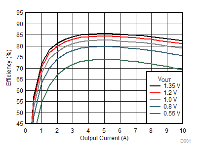
| VIN = 12 V | VG = open |
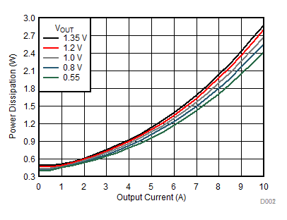
| VIN = 12 V | VG = open |
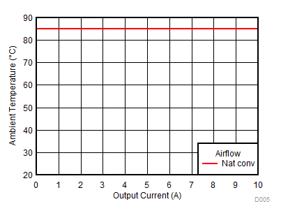
| VIN = 12 V | VOUT = 0.8 V |
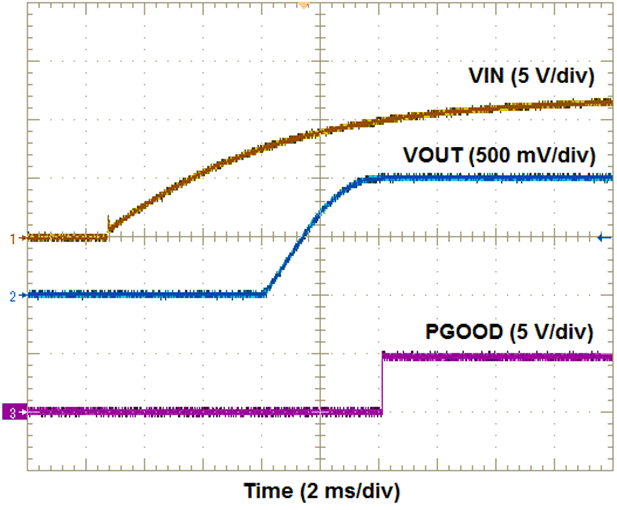
1.
Figure 7. VIN Start-up Waveforms
| VIN = 12 V | VOUT = 1.0 V | IOUT = 1 A |
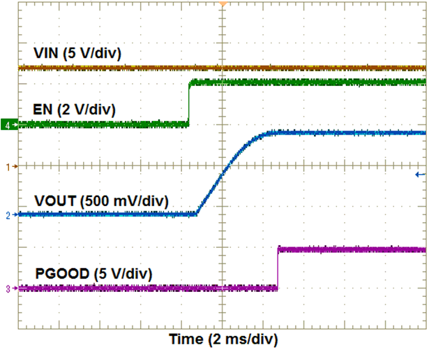
1.
Figure 9. EN Start-up Waveforms
| VIN = 12 V | VOUT = 1.0 V | IOUT = 1 A |
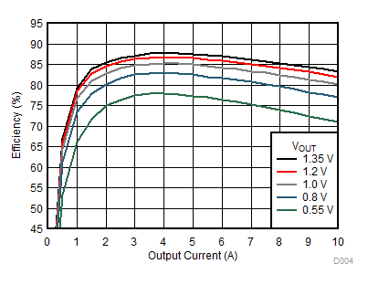
| VIN = 12 V | VG = 5 V |
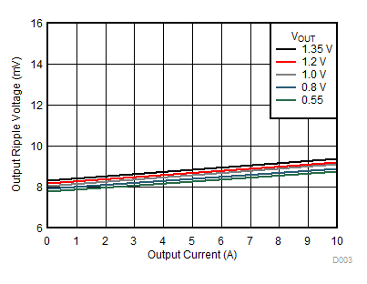
| VIN = 12 V |
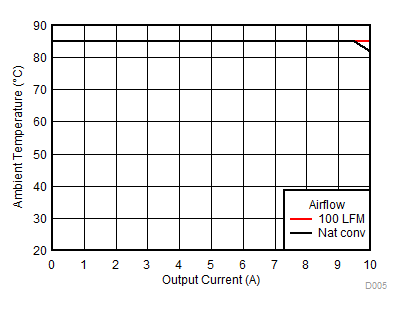
| VIN = 12 V | VOUT = 1.2 V |
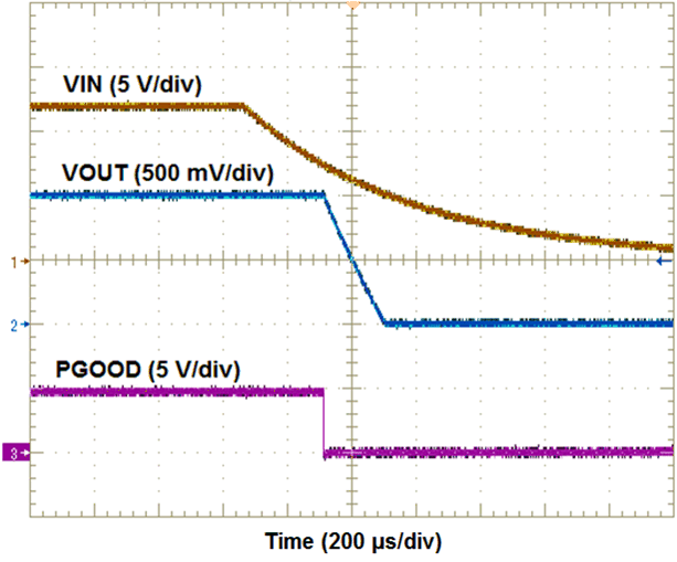
1.
Figure 8. VIN Shut-down Waveforms
| VIN = 12 V | VOUT = 1.0 V | IOUT = 1 A |
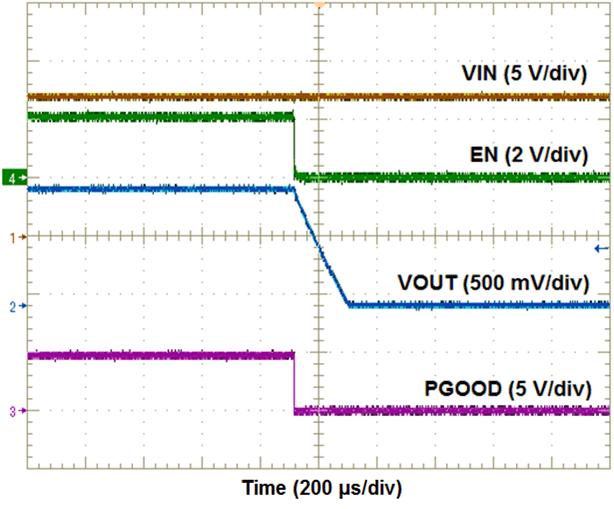
1.
Figure 10. EN Shut-down Waveforms
| VIN = 12 V | VOUT = 1.0 V | IOUT = 1 A |