ZHCSFS5 December 2016 TPSM84A21
PRODUCTION DATA.
- 1 降压稳压器
- 2 应用
- 3 说明
- 4 修订历史记录
- 5 Pin Configuration and Functions
- 6 Specifications
-
7 Detailed Description
- 7.1 Overview
- 7.2 Functional Block Diagram
- 7.3
Feature Description
- 7.3.1 Adjusting the Output Voltage (VADJ)
- 7.3.2 Input and Output Capacitance
- 7.3.3 Transient Response
- 7.3.4 Oscillator Frequency
- 7.3.5 External Clock Syncronization
- 7.3.6 Soft Start
- 7.3.7 Power Good (PGOOD)
- 7.3.8 Gate Driver (VG)
- 7.3.9 Startup into Pre-biased Outputs
- 7.3.10 Thermal Shutdown
- 7.3.11 Overcurrent Protection
- 7.3.12 Output Undervoltage/Overvoltage Protection
- 7.3.13 Enable (EN)
- 7.3.14 Undervoltage Lockout (UVLO)
- 7.4 Device Functional Modes
- 8 Application and Implementation
- 9 Power Supply Recommendations
- 10Layout
- 11器件和文档支持
- 12机械、封装和可订购信息
8 Application and Implementation
NOTE
Information in the following applications sections is not part of the TI component specification, and TI does not warrant its accuracy or completeness. TI’s customers are responsible for determining suitability of components for their purposes. Customers should validate and test their design implementation to confirm system functionality.
8.1 Application Information
The TPSM84A21 is a synchronous series capacitor step down DC-DC power module. It is used to convert a higher DC voltage to a lower DC voltage with a maximum output current of 10 A. The following design procedure can be used to select components for the TPSM84A21. Alternately, the WEBENCH® software may be used to generate complete designs. When generating a design, the WEBENCH software utilizes an iterative design procedure and accesses comprehensive databases of components. Please visit www.ti.com/webench for more details.
8.2 Typical Application
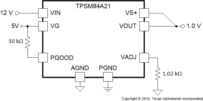
The TPSM84A21 includes both input and output capacitors internal to the device, therefore it only requires a voltage setting resistor and possibly a pull-up resistor on the PGOOD pin in most applications. Figure 17 shows a typical TPSM84A21 schematic with only the minimum required components.
 Figure 17. Typical Application Schematic
8.2.1 Design Requirements
For this design example, use the parameters listed in Table 3 and follow the design procedures below.
Table 3. Design Parameters
| DESIGN PARAMETER | VALUE |
|---|---|
| Input Voltage VIN | 12 V typical |
| Output Voltage VOUT | 1.0 V |
| Output Current Rating | 10 A |
| Key care-abouts | Tight transient response, small footprint, high efficiency, PGOOD signal |
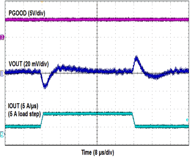
| Transient Response Requirements | ±2% voltage deviation, 5 A load step, 5 A/µs slew rate |
8.2.2 Detailed Design Procedure
8.2.2.1 Setting the Output Voltage
The output voltage of the TPSM84A21 is externally adjustable using a single resistor (RSET). Select the value of RSET from or calculate using Equation 5:

To set the output voltage to 1.0 V, the calculated value for RSET is 1.03 kΩ. The closest E96 value is 1.02 kΩ.
8.2.2.2 Input and Output Capacitance
The TPS84A21 requires no external input or output capacitance to operate. Input and output capacitors can be added to improve ripple or transient response. In this design example, in order to meet the ±2% voltage deviation for a 5-A, 5-A/µs load step, 100 µF of output capacitance is required.
8.2.2.3 Power Good (PGOOD)
Applications requiring voltage rail sequencing can benefit from the PGOOD signal present with the TPSM84A21. The PGOOD pin is an open drain output. When the output voltage is typically between 95% and 105% of the set point, the PGOOD pin pull-down is released and the pin floats, requiring an external pull-up resistor for a high signal. A 10-kΩ pull-up resistor is placed between the PGOOD pin and an external 5V rail.
8.2.2.4 External VG Voltage
The VG supply rail is used to power the internal gate drivers and other internal supply rails used by the controller. For best efficiency, supply an external 5 V to the VG pin, thereby overriding the internal 4.8 V regulator. Expect a 2-3% efficiency improvement by driving the VG pin with an external 5V.
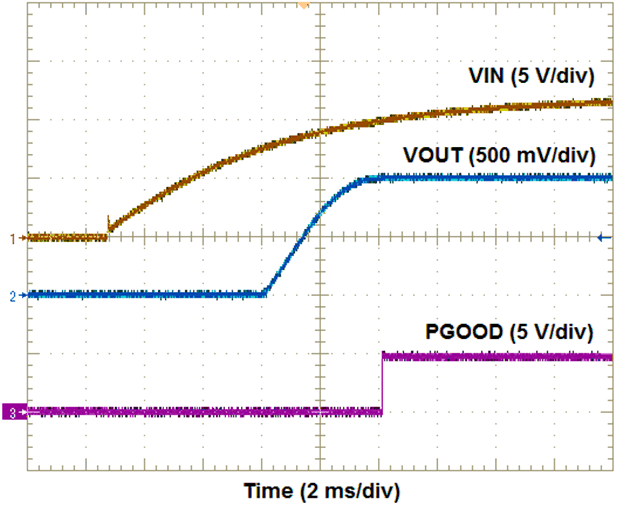
8.2.3 Application Curves

| VIN = 12 V | VOUT = 1.0 V |

| VIN = 12 V | VOUT = 1.0 V | Load Step = 5 A |
| COUT = 100 µF | Slew Rate = 1 A/µs |