ZHCSOO7A August 2021 – November 2021 TPSM8A28 , TPSM8A29
PRODUCTION DATA
- 1 特性
- 2 应用
- 3 说明
- 4 Revision History
- 5 Pin Configuration and Functions
- 6 Specifications
-
7 Detailed Description
- 7.1 Overview
- 7.2 Functional Block Diagram
- 7.3
Feature Description
- 7.3.1 Internal VCC LDO and Using External Bias on VCC Pin
- 7.3.2 Enable
- 7.3.3 Output Voltage Setting
- 7.3.4 Internal Fixed Soft Start and External Adjustable Soft Start
- 7.3.5 External REFIN for Output Voltage Tracking
- 7.3.6 Frequency and Operation Mode Selection
- 7.3.7 D-CAP3™ Control
- 7.3.8 Low-Side FET Zero-Crossing
- 7.3.9 Current Sense and Positive Overcurrent Protection
- 7.3.10 Low-Side FET Negative Current Limit
- 7.3.11 Power Good
- 7.3.12 Overvoltage and Undervoltage Protection
- 7.3.13 Out-Of-Bounds (OOB) Operation
- 7.3.14 Output Voltage Discharge
- 7.3.15 UVLO Protection
- 7.3.16 Thermal Shutdown
- 7.4 Device Functional Modes
-
8 Application and Implementation
- 8.1 Application Information
- 8.2
Typical Application
- 8.2.1 Design Requirements
- 8.2.2
Detailed Design Procedure
- 8.2.2.1 Output Voltage Setting Point
- 8.2.2.2 Choose the Inductor
- 8.2.2.3 Set the Current Limit (TRIP)
- 8.2.2.4 Choose the Output Capacitor
- 8.2.2.5 Choose the Input Capacitors (CIN)
- 8.2.2.6 Soft-Start Capacitor (SS/REFIN Pin)
- 8.2.2.7 EN Pin Resistor Divider
- 8.2.2.8 VCC Bypass Capacitor
- 8.2.2.9 BOOT Capacitor
- 8.2.2.10 PGOOD Pullup Resistor
- 8.2.3 Application Curves
- 9 Power Supply Recommendations
- 10Layout
- 11Device and Documentation Support
- 12Mechanical, Packaging, and Orderable Information
5 Pin Configuration and Functions
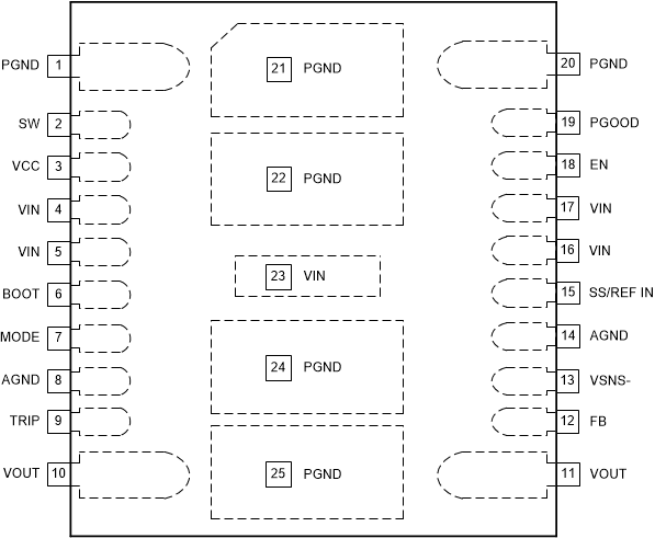
 Figure 5-1 25-Pin B3QFNRDG Package(Top View)
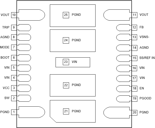
 Figure 5-2 25-Pin B3QFNRDG Package(Bottom View)
Table 5-1 Pin Functions
| PIN | TYPE(1) | DESCRIPTION | |
|---|---|---|---|
| NAME | NO. | ||
| PGND | 1, 20, 21, 22, 24, 25 | G | Power ground of internal low-side MOSFET |
| SW | 2 | O | Output switching terminal of the power converter. No external connection needed. Do not connect. |
| VCC | 3 | I/O | Internal 4.5-V LDO output. Float or connect to an external power supply between 4.75 V and 5.3 V to save the power losses on the internal LDO. The voltage source on this pin powers both the internal circuitry and gate driver. A 1-μF bypass capacitor is built in. No external bypass capacitors are required. |
| VIN | 4, 5, 16, 17, 23 | P | Power-supply input pins for the integrated power MOSFET pair and the internal LDO. Place the decoupling input capacitors from the VIN pins to PGND pins as close as possible. |
| BOOT | 6 | I/O | Supply rail for the high-side gate driver. A boot capacitor is integrated inside module. No external connection is needed. Do not connect. |
| MODE | 7 | I | The MODE pin sets Forced continuous-conduction mode (FCCM) or Skip-mode operation. It also selects the operating frequency by connecting a resistor from the MODE pin to AGND pin. ±1% tolerance resistor is recommended. See Table 7-1 for details. |
| AGND | 8, 14 | G | Ground pin. Reference point for the internal control circuits |
| TRIP | 9 | I/O | Current limit setting pin. Connect a resistor to AGND to set the current limit trip point. ±1% tolerance resistor is highly recommended. See Section 7.3.9 for details on the OCL setting. |
| VOUT | 10, 11 | O | These pins are connected to the output terminal of inductor. Connect these pins to output bypass capacitors. |
| FB | 12 | I | Output voltage feedback input. A resistor divider from the VOUT to VSNS– (tapped to FB pin) sets the output voltage. |
| VSNS– | 13 | I | The return connection for a remote voltage sensing configuration. It is also used as ground for the internal reference. Short to AGND for a single-end sense configuration. |
| SS/REFIN | 15 | I/O | Dual-function pin. Soft-start function: Connecting a capacitor to the VSNS– pin programs the soft-start time. Minimum soft-start time (1.5 ms) is fixed internally. REFIN function: The device always looks at the voltage on this SS/REFIN pin as the reference for the control loop. The internal reference voltage can be overridden by an external DC voltage source on this pin for tracking application. |
| EN | 18 | I | Enable pin. The enable pin turns the DC/DC switching converter on or off. Floating the EN pin before start-up disables the converter. The recommended operating condition for EN pin is maximum 5.5 V. Do not connect the EN pin to the VIN pin directly. |
| PGOOD | 19 | O | Open-drain power-good status signal. When the FB voltage moves outside the specified limits, PGOOD goes low after a 2-µs delay. |
(1) I = Input, O = Output, P = Supply, G = Ground