| VOUT = 0.6
V |
fsw = 600
kHz |
Internal bias |
FCCM |
Figure 8-2 Efficiency
| VOUT = 1.0
V |
fsw = 600
kHz |
Internal bias |
FCCM |
Figure 8-4 Efficiency
| VOUT = 1.8
V |
fsw = 600
kHz |
Internal bias |
FCCM |
Figure 8-6 Efficiency
| VOUT = 3.3
V |
fsw = 600
kHz |
Internal bias |
FCCM |
Figure 8-8 Efficiency
| VIN = 12
V |
VOUT = 1
V |
Internal bias |
FCCM |
Figure 8-10 Efficiency
| VOUT = 0.8
V |
fSW = 600
kHz |
Internal bias |
FCCM |
Figure 8-12 Load Regulation
| VOUT = 1.2
V |
fSW = 600
kHz |
Internal bias |
FCCM |
Figure 8-14 Load Regulation
| VOUT = 2.5
V |
fSW = 600
kHz |
Internal bias |
FCCM |
Figure 8-16 Load Regulation
| VOUT = 5
V |
fSW = 600
kHz |
Internal bias |
FCCM |
Figure 8-18 Load Regulation
| VIN = 12
V |
VOUT = 1.0
V |
Internal bias |
FCCM |
Figure 8-20 Switching
Frequency
| VIN = 12
A |
fSW = 600
kHz |
Internal bias |
FCCM |
Figure 8-22 Switching
Frequency
| VIN = 12
V |
fSW = 600
kHz |
Internal bias |
FCCM |
Figure 8-24 Switching
Frequency
| VOUT = 0.8
V |
fsw = 600
kHz |
Internal bias |
FCCM |
Figure 8-3 Efficiency
| VOUT = 1.2
V |
fsw = 600
kHz |
Internal bias |
FCCM |
Figure 8-5 Efficiency
| VOUT = 2.5
V |
fsw = 600
kHz |
Internal bias |
FCCM |
Figure 8-7 Efficiency
| VOUT = 5
V |
fsw = 600
kHz |
Internal bias |
FCCM |
Figure 8-9 Efficiency
| VOUT = 0.6
V |
fSW = 600
kHz |
Internal bias |
FCCM |
Figure 8-11 Load Regulation
| VOUT = 1.0
V |
fSW = 600
kHz |
Internal bias |
FCCM |
Figure 8-13 Load Regulation
| VOUT = 1.8
V |
fSW = 600
kHz |
Internal bias |
FCCM |
Figure 8-15 Load Regulation
| VOUT = 3.3
V |
fSW = 600
kHz |
Internal bias |
FCCM |
Figure 8-17 Load Regulation
| VOUT = 1.0
V |
IOUT = 5
A |
Internal bias |
fSW = 600
kHz |
FCCM |
Figure 8-19 Line Regulation
| IOUT = 5
A |
fSW = 600
kHz |
Internal bias |
FCCM |
Figure 8-21 Switching
Frequency
| VIN = 12
V |
fSW = 1000
kHz |
Internal bias |
FCCM |
Figure 8-23 Switching
Frequency
| VIN = 12
V |
fSW = 1000
kHz |
Internal bias |
FCCM |
Figure 8-25 Switching
FrequencyIn the following images, all measurements taken with VIN = 12 V,
VOUT = 1 V, fSW = 600 kHz, internal bias, TAMB
= 25°C
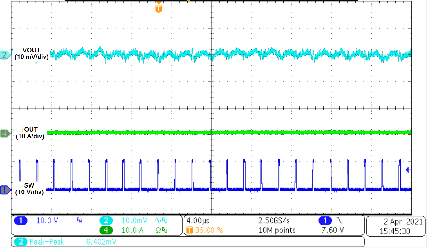
 Figure 8-26 Output Voltage Ripple, VRIPPLE = 6.4
mV
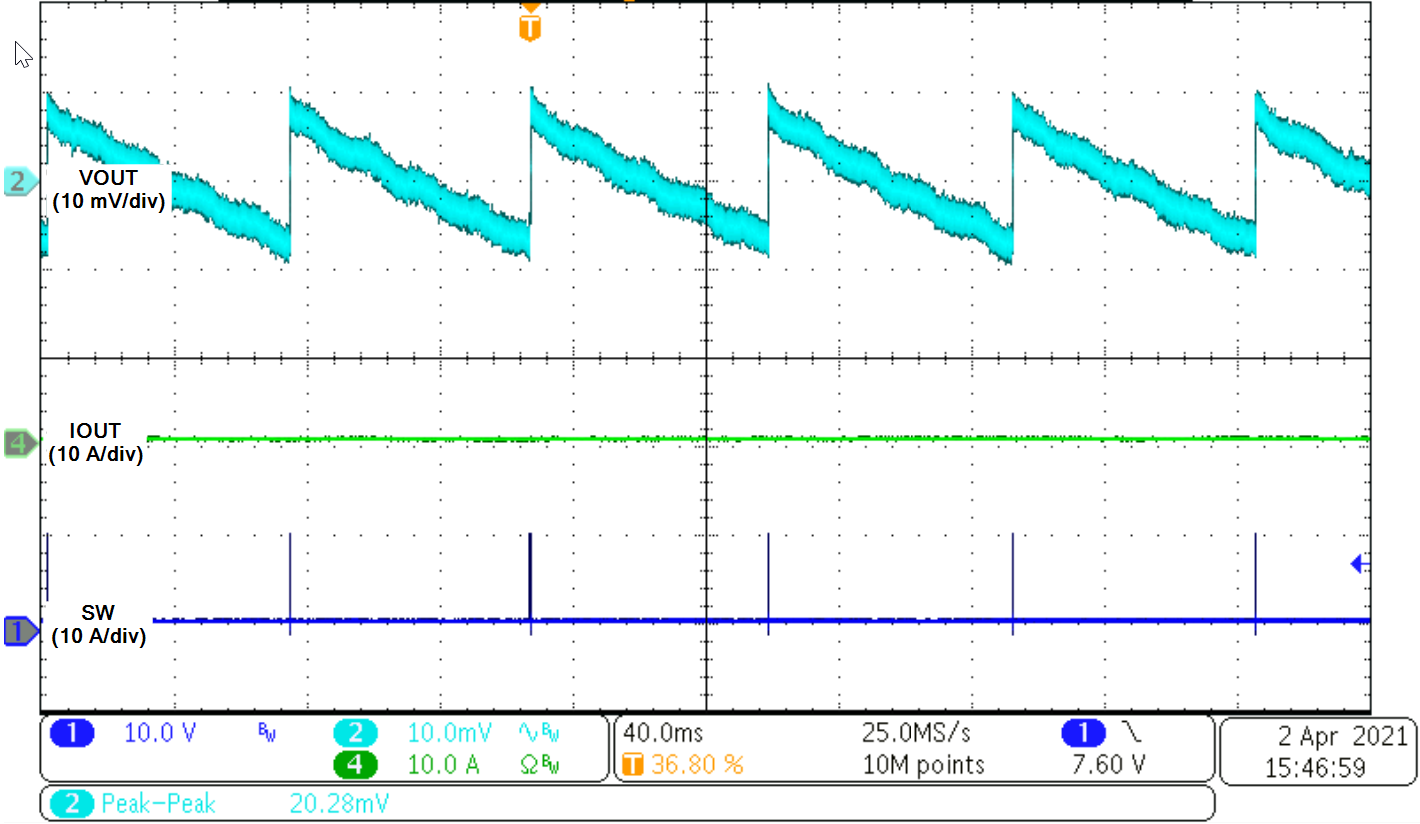
 Figure 8-28 Output Voltage Ripple, VRIPPLE = 20.3
mV
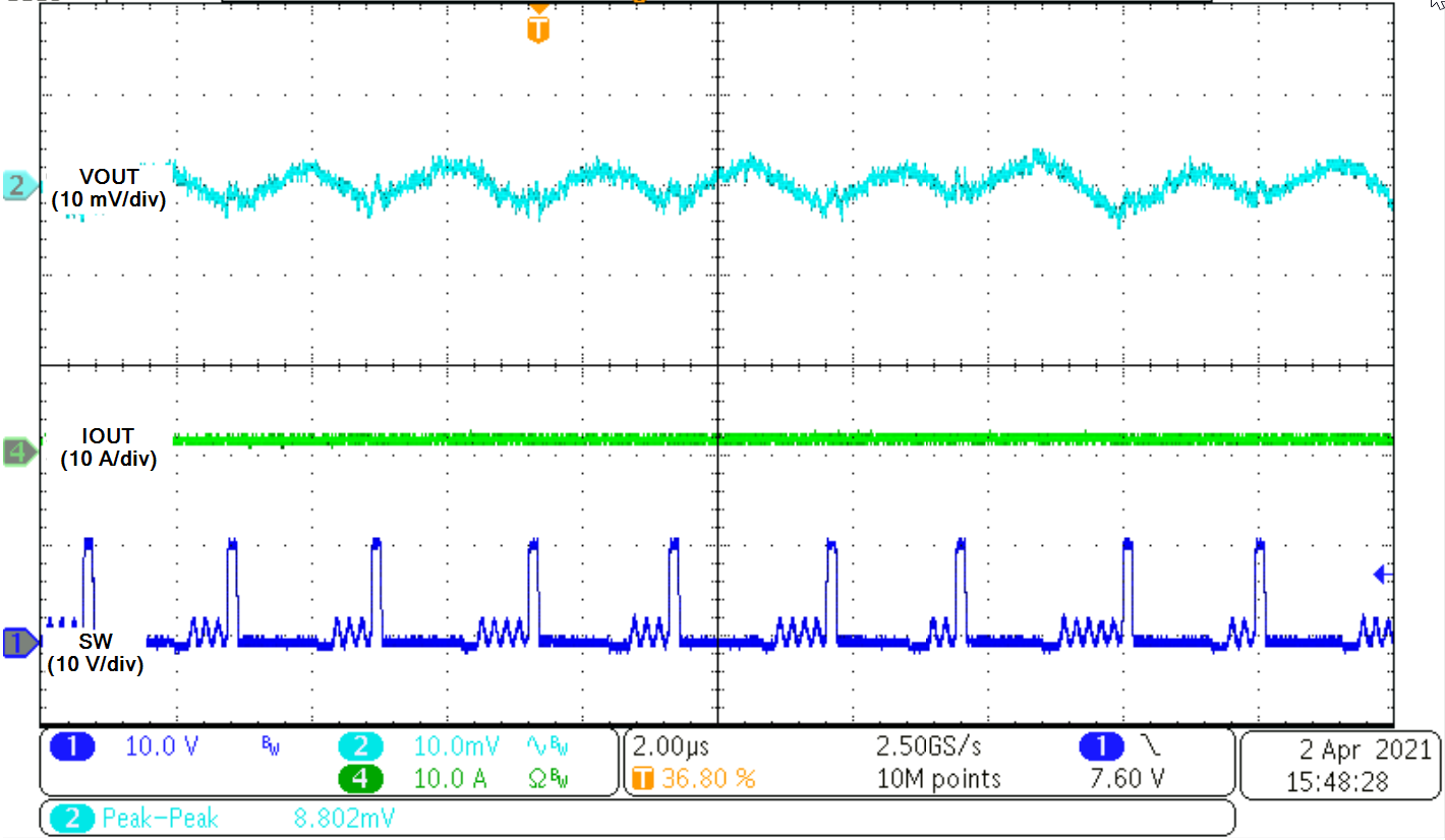
 Figure 8-30 Output Voltage Ripple, VRIPPLE = 8.8
mV
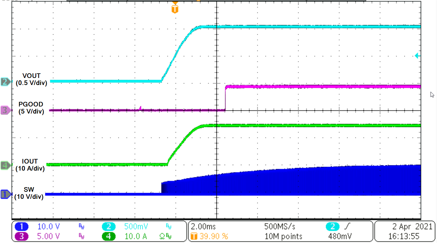
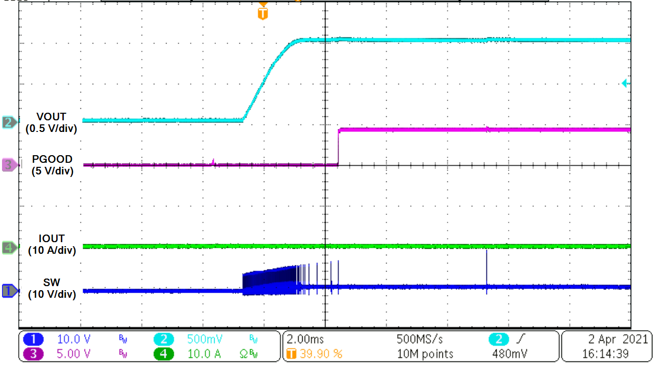
 Figure 8-32 Startup Through VIN (Enable
Floating)
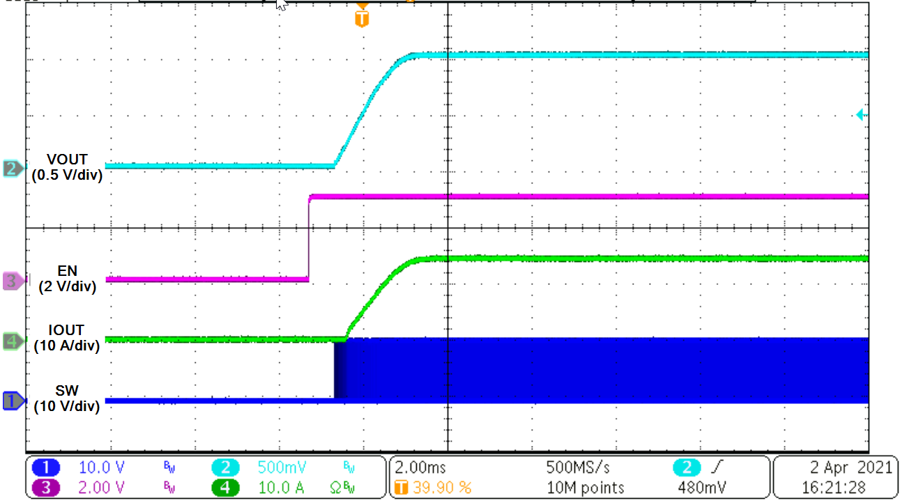
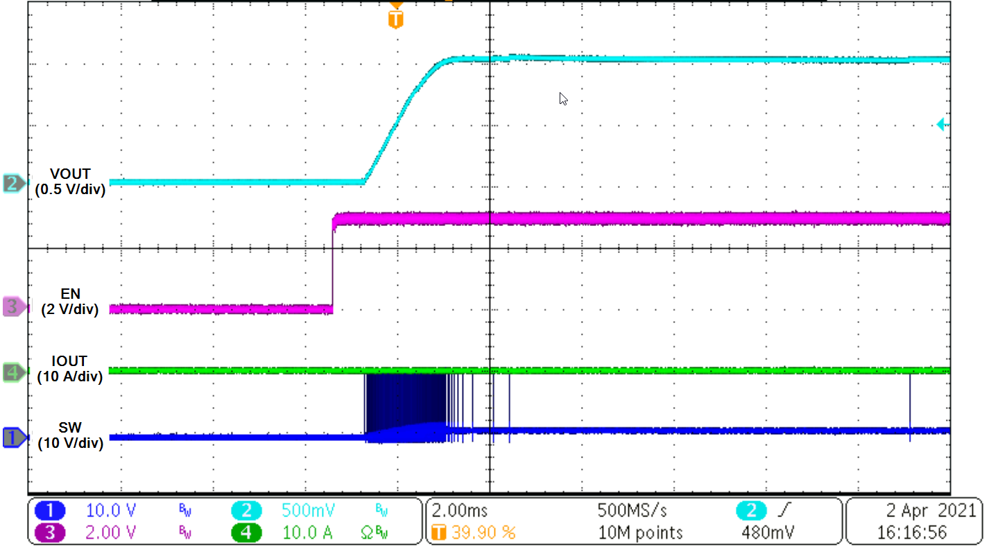
 Figure 8-34 Startup Through Enable
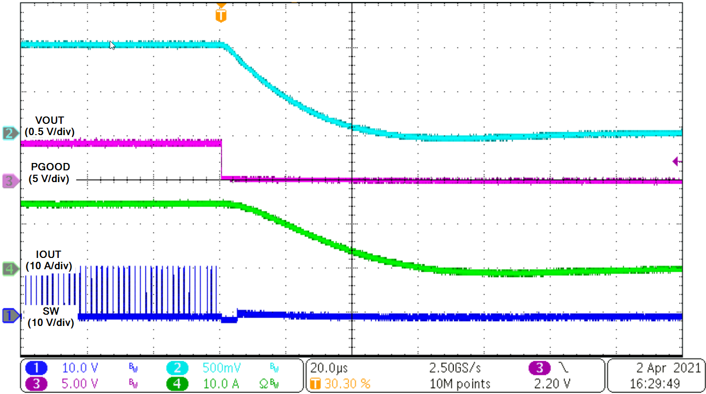
 Figure 8-36 Shutdown Through Enable
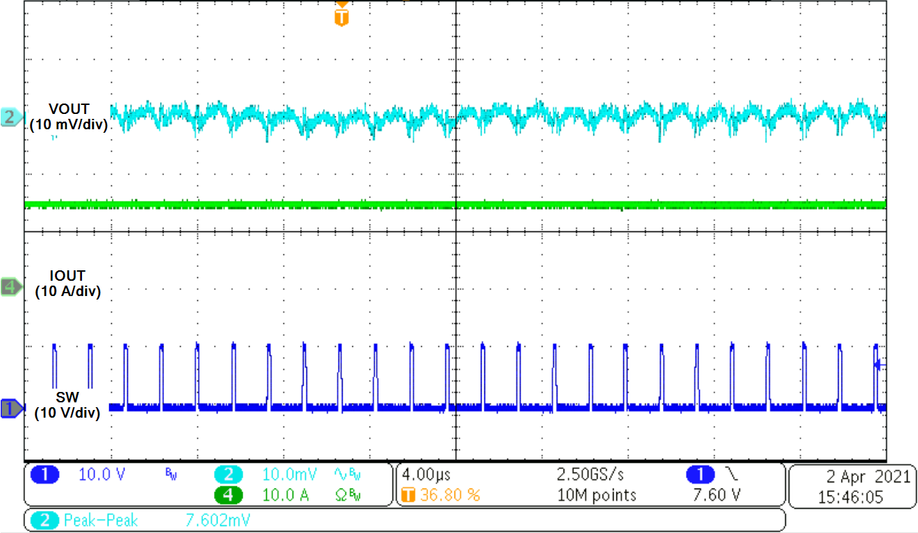
 Figure 8-27 Output Voltage Ripple, VRIPPLE = 7.6
mV
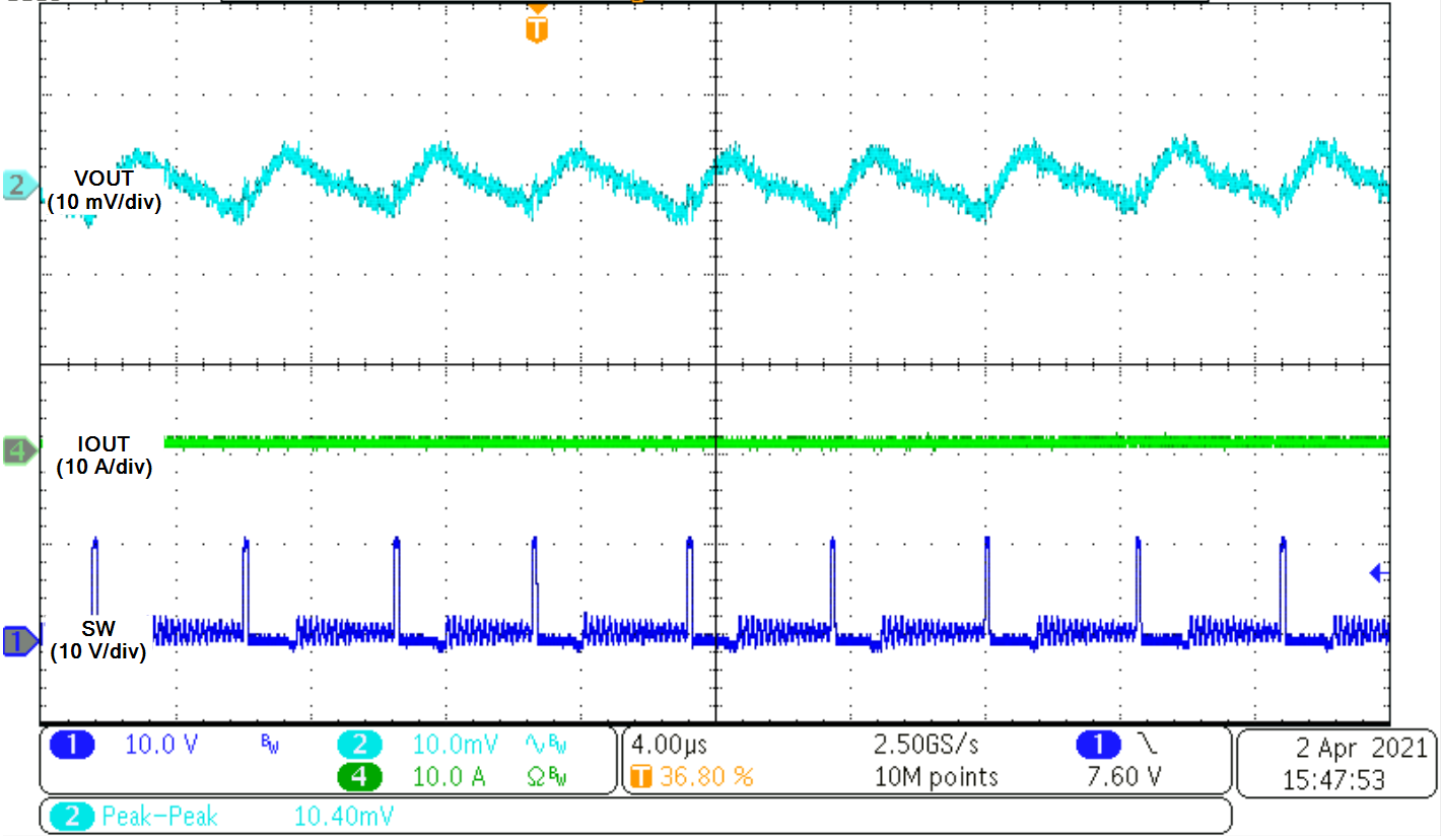
 Figure 8-29 Output Voltage Ripple, VRIPPLE = 10.4
mV
 Figure 8-31 Startup Through VIN (Enable
Floating)
 Figure 8-33 Startup Through Enable
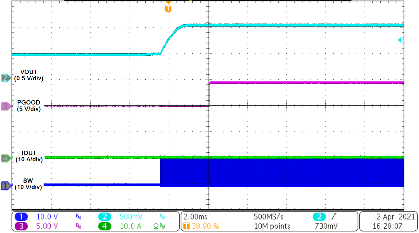
 Figure 8-35 Startup Through Enable into Prebiased Load
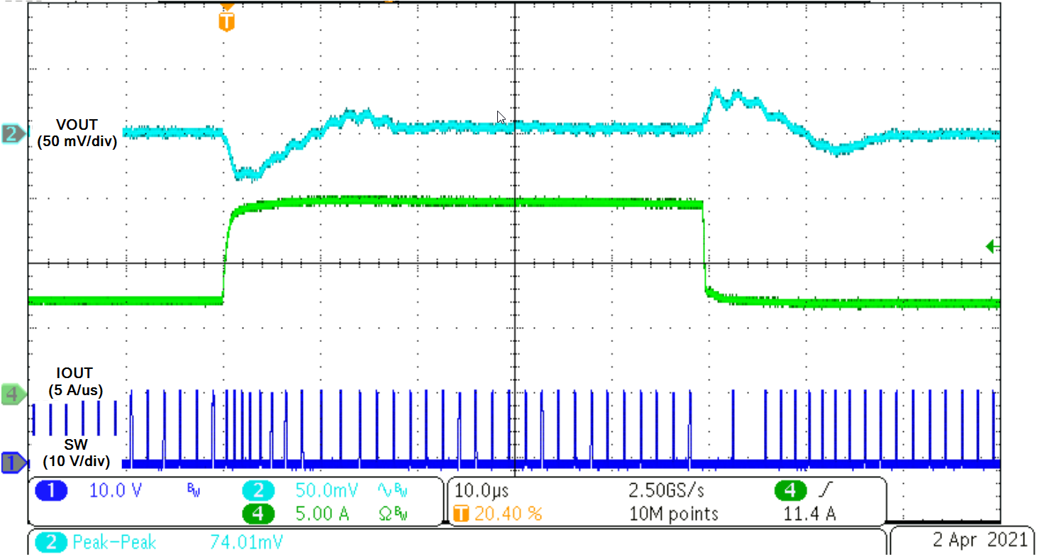
| ISTEP = 7.5
A - 15 A - 7.5 A |
5 A/μs |
Figure 8-37 Transient Response, VPP = 74 mV