ZHCSNL3A December 2021 – November 2023 TPSM8D6C24
PRODUCTION DATA
- 1
- 1 特性
- 2 应用
- 3 说明
- 4 Pin Configuration and Functions
- 5 Specifications
-
6 Detailed Description
- 6.1 Overview
- 6.2 Functional Block Diagram
- 6.3
Feature Description
- 6.3.1 Average Current-Mode Control
- 6.3.2 Linear Regulators
- 6.3.3 AVIN and PVIN Pins
- 6.3.4 Input Undervoltage Lockout (UVLO)
- 6.3.5 Start-Up and Shutdown
- 6.3.6 Differential Sense Amplifier and Feedback Divider
- 6.3.7 Set Output Voltage and Adaptive Voltage Scaling (AVS)
- 6.3.8 Prebiased Output Start-Up
- 6.3.9 Soft Stop and (65h) TOFF_FALL Command
- 6.3.10 Power Good (PGOOD)
- 6.3.11 Set Switching Frequency
- 6.3.12 Frequency Synchronization
- 6.3.13 Loop Follower Detection
- 6.3.14 Current Sensing and Sharing
- 6.3.15 Telemetry
- 6.3.16 Overcurrent Protection
- 6.3.17 Overvoltage and Undervoltage Protection
- 6.3.18 Overtemperature Management
- 6.3.19 Fault Management
- 6.3.20 Back-Channel Communication
- 6.3.21 Switching Node (SW)
- 6.3.22 PMBus General Description
- 6.3.23 PMBus Address
- 6.3.24 PMBus Connections
- 6.4 Device Functional Modes
- 6.5 Programming
- 6.6
Register Maps
- 6.6.1 Conventions for Documenting Block Commands
- 6.6.2 (01h) OPERATION
- 6.6.3 (02h) ON_OFF_CONFIG
- 6.6.4 (03h) CLEAR_FAULTS
- 6.6.5 (04h) PHASE
- 6.6.6 (10h) WRITE_PROTECT
- 6.6.7 (15h) STORE_USER_ALL
- 6.6.8 (16h) RESTORE_USER_ALL
- 6.6.9 (19h) CAPABILITY
- 6.6.10 (1Bh) SMBALERT_MASK
- 6.6.11 (1Bh) SMBALERT_MASK_VOUT
- 6.6.12 (1Bh) SMBALERT_MASK_IOUT
- 6.6.13 (1Bh) SMBALERT_MASK_INPUT
- 6.6.14 (1Bh) SMBALERT_MASK_TEMPERATURE
- 6.6.15 (1Bh) SMBALERT_MASK_CML
- 6.6.16 (1Bh) SMBALERT_MASK_OTHER
- 6.6.17 (1Bh) SMBALERT_MASK_MFR
- 6.6.18 (20h) VOUT_MODE
- 6.6.19 (21h) VOUT_COMMAND
- 6.6.20 (22h) VOUT_TRIM
- 6.6.21 (24h) VOUT_MAX
- 6.6.22 (25h) VOUT_MARGIN_HIGH
- 6.6.23 (26h) VOUT_MARGIN_LOW
- 6.6.24 (27h) VOUT_TRANSITION_RATE
- 6.6.25 (29h) VOUT_SCALE_LOOP
- 6.6.26 (2Bh) VOUT_MIN
- 6.6.27 (33h) FREQUENCY_SWITCH
- 6.6.28 (35h) VIN_ON
- 6.6.29 (36h) VIN_OFF
- 6.6.30 (37h) INTERLEAVE
- 6.6.31 (38h) IOUT_CAL_GAIN
- 6.6.32 (39h) IOUT_CAL_OFFSET
- 6.6.33 (40h) VOUT_OV_FAULT_LIMIT
- 6.6.34 (41h) VOUT_OV_FAULT_RESPONSE
- 6.6.35 (42h) VOUT_OV_WARN_LIMIT
- 6.6.36 (43h) VOUT_UV_WARN_LIMIT
- 6.6.37 (44h) VOUT_UV_FAULT_LIMIT
- 6.6.38 (45h) VOUT_UV_FAULT_RESPONSE
- 6.6.39 (46h) IOUT_OC_FAULT_LIMIT
- 6.6.40 (47h) IOUT_OC_FAULT_RESPONSE
- 6.6.41 (4Ah) IOUT_OC_WARN_LIMIT
- 6.6.42 (4Fh) OT_FAULT_LIMIT
- 6.6.43 (50h) OT_FAULT_RESPONSE
- 6.6.44 (51h) OT_WARN_LIMIT
- 6.6.45 (55h) VIN_OV_FAULT_LIMIT
- 6.6.46 (56h) VIN_OV_FAULT_RESPONSE
- 6.6.47 (58h) VIN_UV_WARN_LIMIT
- 6.6.48 (60h) TON_DELAY
- 6.6.49 (61h) TON_RISE
- 6.6.50 (62h) TON_MAX_FAULT_LIMIT
- 6.6.51 (63h) TON_MAX_FAULT_RESPONSE
- 6.6.52 (64h) TOFF_DELAY
- 6.6.53 (65h) TOFF_FALL
- 6.6.54 (78h) STATUS_BYTE
- 6.6.55 (79h) STATUS_WORD
- 6.6.56 (7Ah) STATUS_VOUT
- 6.6.57 (7Bh) STATUS_IOUT
- 6.6.58 (7Ch) STATUS_INPUT
- 6.6.59 (7Dh) STATUS_TEMPERATURE
- 6.6.60 (7Eh) STATUS_CML
- 6.6.61 (7Fh) STATUS_OTHER
- 6.6.62 (80h) STATUS_MFR_SPECIFIC
- 6.6.63 (88h) READ_VIN
- 6.6.64 (8Bh) READ_VOUT
- 6.6.65 (8Ch) READ_IOUT
- 6.6.66 (8Dh) READ_TEMPERATURE_1
- 6.6.67 (98h) PMBUS_REVISION
- 6.6.68 (99h) MFR_ID
- 6.6.69 (9Ah) MFR_MODEL
- 6.6.70 (9Bh) MFR_REVISION
- 6.6.71 (9Eh) MFR_SERIAL
- 6.6.72 (ADh) IC_DEVICE_ID
- 6.6.73 (AEh) IC_DEVICE_REV
- 6.6.74 (B1h) USER_DATA_01 (COMPENSATION_CONFIG)
- 6.6.75 (B5h) USER_DATA_05 (POWER_STAGE_CONFIG)
- 6.6.76 (D0h) MFR_SPECIFIC_00 (TELEMETRY_CONFIG)
- 6.6.77 (DAh) MFR_SPECIFIC_10 (READ_ALL)
- 6.6.78 (DBh) MFR_SPECIFIC_11 (STATUS_ALL)
- 6.6.79 (DCh) MFR_SPECIFIC_12 (STATUS_PHASE)
- 6.6.80 (E4h) MFR_SPECIFIC_20 (SYNC_CONFIG)
- 6.6.81 (ECh) MFR_SPECIFIC_28 (STACK_CONFIG)
- 6.6.82 (EDh) MFR_SPECIFIC_29 (MISC_OPTIONS)
- 6.6.83 (EEh) MFR_SPECIFIC_30 (PIN_DETECT_OVERRIDE)
- 6.6.84 (EFh) MFR_SPECIFIC_31 (DEVICE_ADDRESS)
- 6.6.85 (F0h) MFR_SPECIFIC_32 (NVM_CHECKSUM)
- 6.6.86 (F1h) MFR_SPECIFIC_33 (SIMULATE_FAULT)
- 6.6.87 (FCh) MFR_SPECIFIC_44 (FUSION_ID0)
- 6.6.88 (FDh) MFR_SPECIFIC_45 (FUSION_ID1)
-
7 Application and Implementation
- 7.1 Application Information
- 7.2
Typical Application
- 7.2.1 Design Requirements
- 7.2.2
Detailed Design Procedure
- 7.2.2.1 Custom Design With WEBENCH® Tools
- 7.2.2.2 Switching Frequency
- 7.2.2.3 Output Voltage Setting (VSEL Pin)
- 7.2.2.4 Compensation Selection (MSEL1 Pin)
- 7.2.2.5 Output Capacitor Selection
- 7.2.2.6 Input Capacitor Selection
- 7.2.2.7 Soft Start, Overcurrent Protection, and Stacking Configuration (MSEL2 Pin)
- 7.2.2.8 Enable and UVLO
- 7.2.2.9 ADRSEL
- 7.2.2.10 BCX_CLK and BCX_DAT
- 7.2.3 Application Curves
- 7.3
Two-Phase Application
- 7.3.1 Design Requirements
- 7.3.2
Two-Phase Detailed Design Procedure
- 7.3.2.1 Switching Frequency
- 7.3.2.2 Output Voltage Setting (VSEL Pin)
- 7.3.2.3 Compensation Selection (MSEL1 Pin)
- 7.3.2.4 Output Capacitor Selection
- 7.3.2.5 Input Capacitor Selection
- 7.3.2.6 GOSNS/Loop Follower Pin of Loop Follower Devices
- 7.3.2.7 Soft Start, Overcurrent Protection, and Stacking Configuration (MSEL2 Pin)
- 7.3.2.8 Enable, UVLO
- 7.3.2.9 VSHARE Pin
- 7.3.2.10 SYNC Pin
- 7.3.2.11 VOSNS Pin of Loop Follower Devices
- 7.3.2.12 Unused Pins of Loop Follower Devices
- 7.3.3 Application Curves
- 7.4 Four-Phase Application
- 7.5 Power Supply Recommendations
- 7.6 Layout
- 8 Device and Documentation Support
- 9 Revision History
- 10Mechanical, Packaging, and Orderable Information
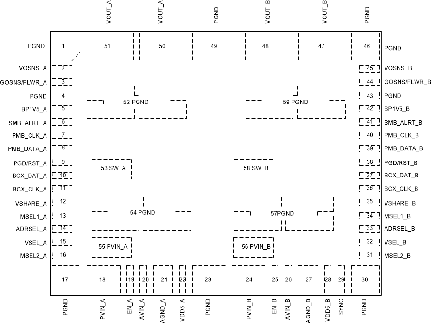
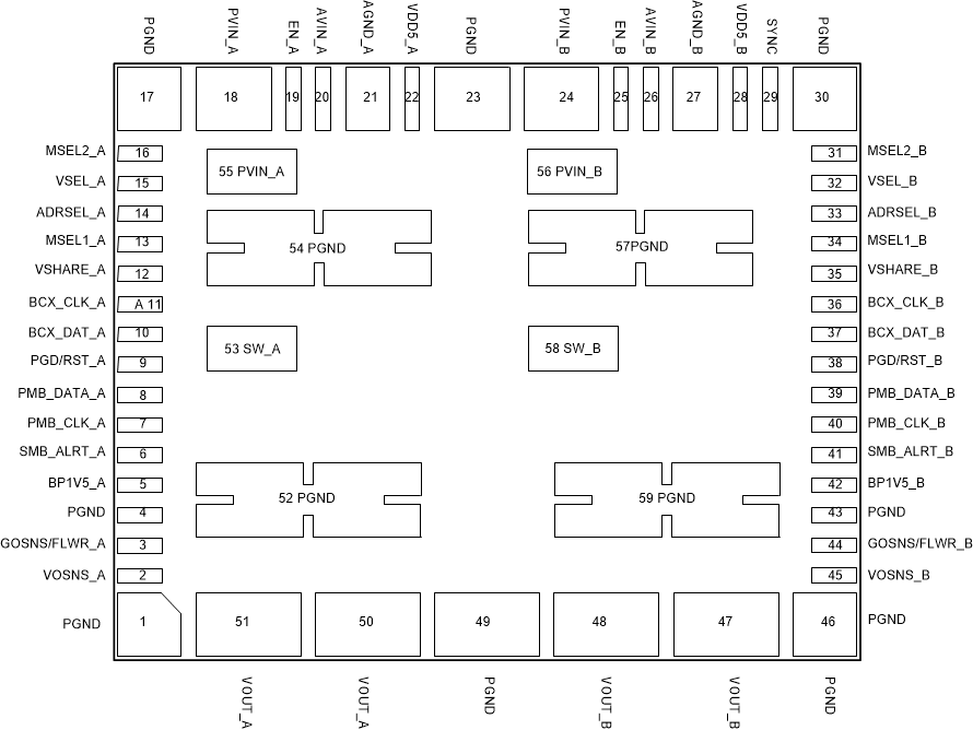
4 Pin Configuration and Functions
 Figure 4-1 59-Pin QFM-MOW Package (Top
View)
 Figure 4-2 59-Pin QFM-MOW Package (Bottom
View)
Figure 4-2 59-Pin QFM-MOW Package (Bottom
View)Table 4-1 Pin Functions
| Pin | Type(1) | Description | |
|---|---|---|---|
| Name | NO. | ||
| PGND | 1, 4, 17, 23, 30, 43, 46, 49, 52, 54, 57, 59 | — | Power stage ground return. Pins 52, 54, 57, and 59 also act as the thermal pad of the device. |
| VOSNS_A | 2 | I | The positive input of the remote sense amplifier. For a standalone device or a loop controller device in a multi-phase configuration, connect the VOSNS pin to the output voltage at the load. For the loop follower device in a multi-phase configuration, the remote sense amplifier is not required for output voltage sensing or regulation and this pin can be left floating. If used to monitor another voltage with the phased READ_VOUT command, VOSNS must be maintained between 0 V and 0.75 V with a < 1-kΩ resistor divider due to the internal resistance to GOSNS, which is connected to BP1V5. |
| VOSNS_B | 45 | ||
| GOSNS/FLWR_A | 3 | I | The negative input of the remote sense amplifier for a loop controller device or pull up high to indicate a loop follower. For a standalone device or a loop controller device in a multi-phase configuration, connect the GOSNS pin to the ground at the load. For the loop follower device in a multi-phase configuration, the GOSNS pin must be pulled up to BP1V5 to indicate the device is a loop follower. |
| GOSNS/FLWR_B | 44 | ||
| BP1V5_A | 5 | O | Output of the 1.5-V internal regulator for MSEL,VSEL, and ADRSEL pins. No external bypassing required. Not designed to power other circuits |
| BP1V5_B | 42 | ||
| SMB_ALRT_A | 6 | O | SMBus alert pin. See the SMBus specification |
| SMB_ALRT_B | 41 | ||
| PMB_CLK_A | 7 | I | PMBus CLK pin. See the Current PMBus Specifications. |
| PMB_CLK_B | 40 | ||
| PMB_DATA_A | 8 | I/O | PMBus DATA pin. See the Current PMBus Specifications. |
| PMB_DATA_B | 39 | ||
| PGD/RST_A | 9 | I/O | Open-drain power good or (21h) VOUT_COMMAND RESET#. As determined by user-programmable RESET# bit in (EDh) MFR_SPECIFIC_29 (MISC_OPTIONS). The default pin function is an open-drain power-good indicator. When configured as RESET#, an internal pullup can be enabled or disabled by the PULLUP# bit in (EDh) MFR_SPECIFIC_29 (MISC_OPTIONS). |
| PGD/RST_B | 38 | ||
| BCX_DATA_A | 10 | I/O | Data for back-channel communications between stacked devices |
| BCX_DATA_B | 37 | ||
| BCX_CLK_A | 11 | I/O | Clock for back-channel communications between stacked devices |
| BCX_CLK_B | 36 | ||
| VSHARE_A | 12 | I/O | Voltage sharing signal for multi-phase operation. For a standalone device, the VSHARE pin must be left floating. VSHARE can by bypassed to AGND with up to 50 pF of capacitance. |
| VSHARE_B | 35 | ||
| MSEL1_A | 13 | I | Connect this pin to a resistor divider between BP1V5and AGND for different options of switching frequency and internal compensation parameters. See the Programming MSEL1 section. |
| MSEL1_B | 34 | ||
| ADRSEL_A | 14 | I | Connect this pin to a resistor divider between BP1V5 and AGND for different options of PMBus addresses and frequency sync (including determination of SYNC pin as SYNCIN or SYNCOUT function). See the Programming ADRSEL section. |
| ADRSEL_B | 33 | ||
| VSEL_A | 15 | I | Connect this pin to a resistor divider between BP1V5 and AGND for different options of internal voltage feedback dividers and default output voltage. See Programming VSEL. |
| VSEL_B | 32 | ||
| MSEL2_A | 16 | I | Connect this pin to a resistor divider between BP1V5 and AGND for different options of soft-start time, overcurrent fault limit, and multiphase information. See the Programming MSEL2 or Programming MSEL2 for a Loop Follower Device (GOSNS Tied to BP1V5) sections for a loop follower device (GOSNS tied to BP1V5) if GOSNS is tied to BP1V5. |
| MSEL2_B | 31 | ||
| EN/UVLO_A | 19 | I | Enable switching as the PMBus CONTROL pin. EN/UVLO can also be connected to a resistor divider to program input voltage UVLO. |
| EN/UVLO_B | 25 | ||
| PVIN_A | 18, 55 | I | Input power to the power stage. Low-impedance bypassing of these pins to PGND is critical. PVIN to PGND must be bypassed with X5R or better ceramic capacitors rated for at least 1.5× the maximum PVIN voltage. |
| PVIN_B | 24, 56 | ||
| AVIN_A | 20 | I | Input power to the controller |
| AVIN_B | 26 | ||
| AGND_A | 21 | — | Analog ground return for controller. Connect the AGND pin directly to the thermal pad on the PCB board. |
| AGND_B | 27 | ||
| VDD5_A | 22 | O | Output of the 5-V internal regulator. A bypassing capacitor is integrated and no external bypassing is required. |
| VDD5_B | 28 | ||
| SYNC | 29 | I/O | For frequency synchronization, this pin can be programmed as SYNC IN or SYNC OUT pin by the ADRSEL pin or the (E4h) MFR_SPECIFIC_20 (SYNC_CONFIG) PMBus command. SYNC is tied together internally for phase A and B. SYNC pin can be left floating when using module in single-phase configuration. |
| VOUT_A | 50, 51 | O | Output of each channel. Connect to output bypass capacitors to this pin. |
| VOUT_B | 47, 48 | ||
| Thermal Pad | 52, 54, 57, 59 | — | The thermal pad is the PGND pin made with a large area of copper to improve thermal conductivity to PCB. The thermal pad must have adequate solder coverage for best thermal performance. |
| SW_A | 53 | I/O | Switched power output of the device. Connect the output averaging filter and bootstrap to this group of pins if needed. |
| SW_B | 58 | ||
(1) I = input, O = output