SLWS213A January 2010 – November 2015 TRF370417
PRODUCTION DATA.
- 1 Features
- 2 Applications
- 3 Description
- 4 Revision History
- 5 Pin Configuration and Functions
- 6 Specifications
- 7 Detailed Description
- 8 Application and Implementation
- 9 Power Supply Recommendations
- 10Layout
- 11Device and Documentation Support
- 12Mechanical, Packaging, and Orderable Information
封装选项
机械数据 (封装 | 引脚)
- RGE|24
散热焊盘机械数据 (封装 | 引脚)
- RGE|24
订购信息
11 Device and Documentation Support
11.1 Device Support
11.1.1 Device Nomenclature
-
Adjusted (Optimized) Carrier Feedthrough This differs from the unadjusted suppression number in that the baseband input dc offsets are iteratively adjusted around their theoretical value of VCM to yield the maximum suppression of the LO component in the output spectrum. This is measured in dBm.
-
Adjusted (Optimized) Sideband Suppression This differs from the unadjusted sideband suppression in that the gain and phase of the baseband inputs are iteratively adjusted around their theoretical values to maximize the amount of sideband suppression. This is measured in dBc.
-
Suppressions Over Temperature This specification assumes that the user has gone though the optimization process for the suppression in question, and set the optimal settings for the I, Q inputs. This specification then measures the suppression when temperature conditions change after the initial calibration is done.
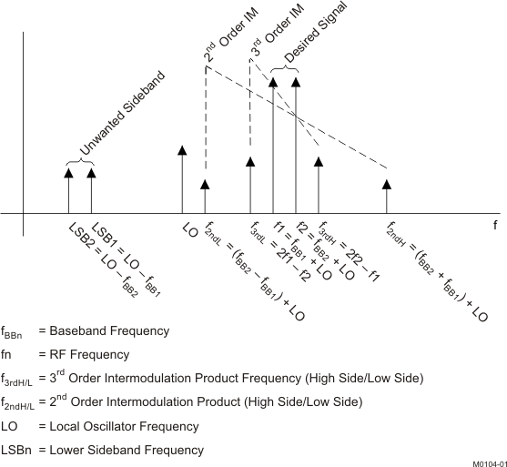
Figure 45 shows a simulated output and illustrates the respective definitions of various terms used in this data sheet.
 Figure 45. Graphical Illustration of Common Terms
-
Unadjusted Carrier Feedthrough This specification measures the amount by which the local oscillator component is suppressed in the output spectrum of the modulator. If the common-mode voltage at each of the baseband inputs is exactly the same and there was no dc imbalance introduced by the modulator, the LO component would be naturally suppressed. DC offset imbalances in the device allow some of the LO component to feed through to the output. Because this phenomenon is independent of the RF output power and the injected LO input power, the parameter is expressed in absolute power, dBm.
-
Unadjusted Sideband Suppression This specification measures the amount by which the unwanted sideband of the input signal is suppressed in the output of the modulator, relative to the wanted sideband. If the amplitude and phase within the I and Q branch of the modulator were perfectly matched, the unwanted sideband (or image) would be naturally suppressed. Amplitude and phase imbalance in the I and Q branches results in the increase of the unwanted sideband. This parameter is measured in dBc relative to the desired sideband.
11.2 Documentation Support
11.2.1 Related Documentation
For related documentation, see the documents that follow:
11.3 Community Resources
The following links connect to TI community resources. Linked contents are provided "AS IS" by the respective contributors. They do not constitute TI specifications and do not necessarily reflect TI's views; see TI's Terms of Use.
-
TI E2E™ Online Community TI's Engineer-to-Engineer (E2E) Community. Created to foster collaboration among engineers. At e2e.ti.com, you can ask questions, share knowledge, explore ideas and help solve problems with fellow engineers.
-
Design Support TI's Design Support Quickly find helpful E2E forums along with design support tools and contact information for technical support.
11.4 Trademarks
E2E is a trademark of Texas Instruments.
All other trademarks are the property of their respective owners.
11.5 Electrostatic Discharge Caution

These devices have limited built-in ESD protection. The leads should be shorted together or the device placed in conductive foam during storage or handling to prevent electrostatic damage to the MOS gates.
11.6 Glossary
SLYZ022 — TI Glossary.
This glossary lists and explains terms, acronyms, and definitions.