SLWS213A January 2010 – November 2015 TRF370417
PRODUCTION DATA.
- 1 Features
- 2 Applications
- 3 Description
- 4 Revision History
- 5 Pin Configuration and Functions
- 6 Specifications
- 7 Detailed Description
- 8 Application and Implementation
- 9 Power Supply Recommendations
- 10Layout
- 11Device and Documentation Support
- 12Mechanical, Packaging, and Orderable Information
封装选项
机械数据 (封装 | 引脚)
- RGE|24
散热焊盘机械数据 (封装 | 引脚)
- RGE|24
订购信息
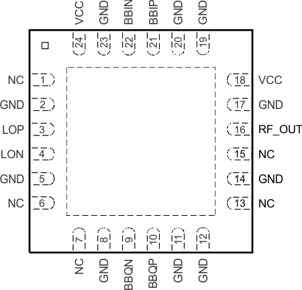
5 Pin Configuration and Functions
RGE Package
24-Pin VQFN With Exposed Thermal Pad
Top View

Pin Functions
| PIN | I/O | DESCRIPTION | |
|---|---|---|---|
| NAME | NO. | ||
| BBIN | 22 | I | In-phase negative input |
| BBIP | 21 | I | In-phase positive input |
| BBQN | 9 | I | Quadrature-phase negative input |
| BBQP | 10 | I | Quadrature-phase positive input |
| GND | 2, 5, 8, 11, 12, 14, 17, 19, 20, 23 | — | Ground |
| LON | 4 | I | Local oscillator (LO) negative input |
| LOP | 3 | I | Local oscillator (LO) positive input |
| NC | 1, 6, 7, 13, 15 | — | No connect |
| RF_OUT | 16 | O | RF output |
| VCC | 18, 24 | — | Power supply |