SLWS223B August 2011 – November 2015 TRF3705
PRODUCTION DATA.
- 1 Features
- 2 Applications
- 3 Description
- 4 Revision History
- 5 Pin Configuration and Functions
-
6 Specifications
- 6.1 Absolute Maximum Ratings
- 6.2 ESD Ratings
- 6.3 Recommended Operating Conditions
- 6.4 Thermal Information
- 6.5 Electrical Characteristics: General
- 6.6 Electrical Characteristics
- 6.7 Typical Characteristics: Single-Tone Baseband
- 6.8 Typical Characteristics: Two-Tone Baseband
- 6.9 Typical Characteristics: Two-Tone Baseband, Mid-Band Calibration
- 6.10 Typical Characteristics: No Baseband
- 6.11 Typical Characteristics: Two-Tone Baseband
- 7 Detailed Description
- 8 Application and Implementation
- 9 Power Supply Recommendations
- 10Layout
- 11Device and Documentation Support
- 12Mechanical, Packaging, and Orderable Information
封装选项
机械数据 (封装 | 引脚)
- RGE|24
散热焊盘机械数据 (封装 | 引脚)
- RGE|24
订购信息
10 Layout
Populated RoHS-compliant evaluation boards are available for testing the TRF3705 as a stand-alone device. Contact your local TI representative for information on ordering these evaluation modules, or see the TRF3705 product folder on the TI website. In addition, the TRF3705 can be evaluated with the DAC348x (quad/dual 16-bit, 1.25GSPS) EVM driving the baseband inputs through a seamless interface at 0.25V common-mode voltage.
10.1 Layout Guidelines
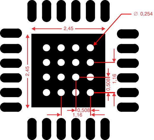
The TRF3705 device is fitted with a ground slug on the back of the package that must be soldered to the printed circuit board (PCB) ground with adequate ground vias to ensure a good thermal and electrical connection. The recommended via pattern and ground pad dimensions are shown in Figure 76. The recommended via diameter is 10 mils (0.10 in or 0,25 mm). The ground pins of the device can be directly tied to the ground slug pad for a low-inductance path to ground. Additional ground vias may be added if space allows.
Decoupling capacitors at each of the supply pins are strongly recommended. The value of these capacitors should be chosen to provide a low-impedance RF path to ground at the frequency of operation. Typically, the value of these capacitors is approximately 10 pF or lower.
The device exhibits symmetry with respect to the quadrature input paths. It is recommended that the PCB layout maintain this symmetry in order to ensure that the quadrature balance of the device is not impaired. The I/Q input traces should be routed as differential pairs and the respective lengths all kept equal to each other. On the RF traces, maintain proper trace widths to keep the characteristic impedance of the RF traces at a nominal 50 Ω.
10.2 Layout Example

NOTE:
Dimensions are in millimeters (mm).