SLWS224E August 2010 – January 2016 TRF372017
PRODUCTION DATA.
- 1 Features
- 2 Applications
- 3 Description
- 4 Revision History
- 5 Pin Configuration and Functions
- 6 Specifications
-
7 Detailed Description
- 7.1 Overview
- 7.2 Functional Block Diagram
- 7.3
Feature Description
- 7.3.1 Integer and Fractional Mode Selection
- 7.3.2 Description of PLL Structure
- 7.3.3 Fractional Mode Setup
- 7.3.4 Selecting the VCO and VCO Frequency Control
- 7.3.5 External VCO
- 7.3.6 VCO Test Mode
- 7.3.7 Lock Detect
- 7.3.8 Tx Divider
- 7.3.9 LO Divider
- 7.3.10 Mixer
- 7.3.11 Disabling Outputs
- 7.3.12 Power Supply Distribution
- 7.3.13 Carrier Feedthrough Cancellation
- 7.3.14 Internal Baseband Bias Voltage Generation
- 7.4 Device Functional Modes
- 7.5 Register Maps
- 8 Application and Implementation
- 9 Power Supply Recommendations
- 10Layout
- 11Device and Documentation Support
- 12Mechanical, Packaging, and Orderable Information
10 Layout
10.1 Layout Guidelines
Layout of the application board significantly impacts the analog performance of the TRF372017 device. Noise and high-speed signals must be prevented from leaking onto power-supply pins or analog signals. Follow these recommendations:
- Place supply decoupling capacitors physically close to the device, on the same side of the board. Each supply pin must be isolated with a ferrite bead.
- Maintain a continuous ground plane in the vicinity of the device and as return paths for all high-speed signal lines. Place reference plane vias or decoupling capacitors near any signal line reference transition.
- The pad on the bottom of the device must be electrically grounded. Connect GND pins directly to the pad on the surface layer. Connect the GND pins and pad directly to surface ground where possible.
- Power planes must not overlap each other or high-speed signal lines.
- Isolate REF_IN routing from loop filter lines, control lines, and other high-speed lines.
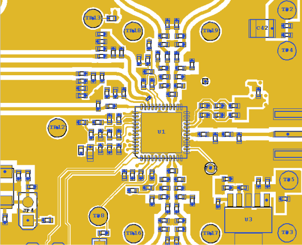
See Figure 95 for an example of critical component layout (for the top PCB layer).
10.2 Layout Example
 Figure 95. Critical Layout of the TRF372017 EVM Board