SLWS224E August 2010 – January 2016 TRF372017
PRODUCTION DATA.
- 1 Features
- 2 Applications
- 3 Description
- 4 Revision History
- 5 Pin Configuration and Functions
- 6 Specifications
-
7 Detailed Description
- 7.1 Overview
- 7.2 Functional Block Diagram
- 7.3
Feature Description
- 7.3.1 Integer and Fractional Mode Selection
- 7.3.2 Description of PLL Structure
- 7.3.3 Fractional Mode Setup
- 7.3.4 Selecting the VCO and VCO Frequency Control
- 7.3.5 External VCO
- 7.3.6 VCO Test Mode
- 7.3.7 Lock Detect
- 7.3.8 Tx Divider
- 7.3.9 LO Divider
- 7.3.10 Mixer
- 7.3.11 Disabling Outputs
- 7.3.12 Power Supply Distribution
- 7.3.13 Carrier Feedthrough Cancellation
- 7.3.14 Internal Baseband Bias Voltage Generation
- 7.4 Device Functional Modes
- 7.5 Register Maps
- 8 Application and Implementation
- 9 Power Supply Recommendations
- 10Layout
- 11Device and Documentation Support
- 12Mechanical, Packaging, and Orderable Information
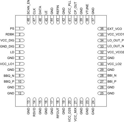
5 Pin Configuration and Functions
RGZ Package
48-Pin VQFN
Top View

Pin Functions
| PIN | I/O | DESCRIPTION | |
|---|---|---|---|
| NAME | NO. | ||
| BBI_P | 27 | I | Base-band in-phase input: positive terminal. Internal 5 kΩ to VCM generator. If VCM is internally generated (PWD_BB_VCM = 0), external AC coupling caps and 100-Ω differential termination to BBI_N is required. |
| BBI_N | 28 | I | Base-band in-phase input: negative terminal. Internal 5 kΩ to VCM generator. If VCM is internally generated (PWD_BB_VCM = 0), external AC coupling caps and 100-Ω differential termination to BBI_P is required. |
| BBQ_N | 9 | I | Base-band in-quadrature input: negative terminal. Internal 5 kΩ to VCM generator. If VCM is internally generated (PWD_BB_VCM = 0), external AC coupling caps and 100-Ω differential termination to BBQ_P is required. |
| BBQ_P | 10 | I | Base-band in-quadrature input: positive terminal. Internal 5 kΩ to VCM generator. If VCM is internally generated (PWD_BB_VCM = 0), external AC coupling caps and 100-Ω differential termination to BBQ_N is required. |
| CLK | 47 | I | SPI clock input. Digital input. High impedance. |
| CP_OUT | 40 | O | Charge pump output |
| DATA | 46 | I | SPI data input. Digital input. High impedance. |
| EXT_VCO | 36 | I | External local oscillator input. High impedance. Normally AC-coupled. |
| GND | 6, 8, 11, 12, 13, 15, 16, 17, 19, 22, 23, 24, 25, 26, 29, 31, 37, 39, 42, 44 | — | Ground |
| GND_DIG | 4 | — | Digital ground |
| LD | 5 | O | PLL lock detect output, as configured by MUX_CTRL. Digital output pins can source or sink up to 8 mA of current. |
| LE | 45 | I | SPI latch enable. Digital input. High impedance. |
| LO_OUT_N | 33 | O | Local oscillator output: negative terminal. Open collector output. A pullup is required. Normally AC-coupled. |
| LO_OUT_P | 34 | O | Local oscillator output: positive terminal. Open collector output. A pullup is required. Normally AC-coupled. |
| PS | 1 | I | Power saving mode enable (Low = normal mode; High = power saving mode) |
| RDBK | 2 | O | SPI internal registers readback output. Digital output pins can source or sink up to 8 mA of current. |
| REFIN | 43 | I | Reference clock input. High impedance. Normally AC-coupled. |
| RFOUT | 18 | O | RF output. Internally matched to 50-Ω output. Normally AC-coupled. |
| RSVD | 14 | — | Reserved. Normally open. |
| SCAN_EN | 48 | I | Internal testing mode digital input. Connect to ground in normal operation |
| VCC_D2S | 20 | — | 5-V modulator output buffer power supply |
| VCC_DIG | 3 | — | 3.3-V digital power supply |
| VCC_LO1 | 7 | — | 3.3-V Tx path local oscillator chain power supply |
| VCC_LO2 | 30 | — | 3.3-V output local oscillator chain power supply |
| VCC_MIX | 21 | — | 5-V modulator power supply |
| VCC_PLL | 41 | — | 3.3-V PLL power supply |
| VCC_VCO1 | 35 | — | 3.3-V VCO power supply |
| VCC_VCO2 | 32 | — | 3.3-V to 5-V VCO power supply |
| VTUNE | 38 | I | VCO control voltage input |