SLWS224E August 2010 – January 2016 TRF372017
PRODUCTION DATA.
- 1 Features
- 2 Applications
- 3 Description
- 4 Revision History
- 5 Pin Configuration and Functions
- 6 Specifications
-
7 Detailed Description
- 7.1 Overview
- 7.2 Functional Block Diagram
- 7.3
Feature Description
- 7.3.1 Integer and Fractional Mode Selection
- 7.3.2 Description of PLL Structure
- 7.3.3 Fractional Mode Setup
- 7.3.4 Selecting the VCO and VCO Frequency Control
- 7.3.5 External VCO
- 7.3.6 VCO Test Mode
- 7.3.7 Lock Detect
- 7.3.8 Tx Divider
- 7.3.9 LO Divider
- 7.3.10 Mixer
- 7.3.11 Disabling Outputs
- 7.3.12 Power Supply Distribution
- 7.3.13 Carrier Feedthrough Cancellation
- 7.3.14 Internal Baseband Bias Voltage Generation
- 7.4 Device Functional Modes
- 7.5 Register Maps
- 8 Application and Implementation
- 9 Power Supply Recommendations
- 10Layout
- 11Device and Documentation Support
- 12Mechanical, Packaging, and Orderable Information
6 Specifications
6.1 Absolute Maximum Ratings
over operating free-air temperature range (unless otherwise noted)(1)(3)| MIN | MAX | UNIT | ||
|---|---|---|---|---|
| Supply voltage(2) | –0.3 | 5.5 | V | |
| Digital I/O voltage | –0.3 | VCC + 0.5 | V | |
| TJ | Operating virtual junction temperature | –40 | 150 | °C |
| TA | Operating ambient temperature | –40 | 85 | °C |
| Tstg | Storage temperature | –40 | 150 | °C |
(1) Stresses beyond those listed under Absolute Maximum Ratings may cause permanent damage to the device. These are stress ratings only, which do not imply functional operation of the device at these or any other conditions beyond those indicated under Recommended Operating Conditions. Exposure to absolute-maximum-rated conditions for extended periods may affect device reliability.
(2) All voltage values are with respect to network ground terminal.
(3) ESD rating not valid for RF sensitive pins.
6.2 Recommended Operating Conditions
| MIN | NOM | MAX | UNIT | ||
|---|---|---|---|---|---|
| VCC5V | 5-V power supply voltage | 4.5 | 5 | 5.5 | V |
| VCC3V | 3.3-V power supply voltage | 3 | 3.3 | 3.6 | V |
| VCC_VCO2 | 3.3-V to 5-V power supply voltage | 3 | 3.3 | 5.5 | V |
| TA | Operating ambient temperature | –40 | 85 | °C | |
| TJ | Operating virtual junction temperature | –40 | 125 | °C | |
6.3 Thermal Information
| THERMAL METRIC(1) | TRF372017 | UNIT | |
|---|---|---|---|
| RGZ (VQFN) | |||
| 48 PINS | |||
| RθJA | Junction-to-ambient thermal resistance | 30.0 | °C/W |
| RθJC(top) | Junction-to-case (top) thermal resistance | 10.0 | °C/W |
| RθJB | Junction-to-board thermal resistance | 8.0 | °C/W |
| ψJT | Junction-to-top characterization parameter | 0.5 | °C/W |
| ψJB | Junction-to-board characterization parameter | 7.0 | °C/W |
| RθJC(bot) | Junction-to-case (bottom) thermal resistance | 0.5 | °C/W |
(1) For more information about traditional and new thermal metrics, see the Semiconductor and IC Package Thermal Metrics application report, SPRA953.
6.4 Electrical Characteristics
VCC5V = 5 V, VCC3V = 3.3 V, VCC_VCO2 = 3.3 V, TA = 25°C, internal LO, internal VCM (unless otherwise noted)| PARAMETER | TEST CONDITIONS | MIN | TYP | MAX | UNIT | |
|---|---|---|---|---|---|---|
| DC PARAMETERS | ||||||
| ICC | Total supply current, LO on(1) | 3.3-V power supply, LO on | 200 | 250 | mA | |
| 5-V power supply, LO on | 117 | 148 | mA | |||
| Supply current, LO on(1) | VCC_DIG, LO on | 3 | 5 | mA | ||
| VCC_LO1 and VCC_LO2 | 121 | 130 | mA | |||
| VCC_D2S | 43 | 60 | mA | |||
| VCC_MIX | 74 | 90 | mA | |||
| VCC_VCO1 | 20 | 28 | mA | |||
| VCC_VCO2 | 17 | 20 | ||||
| LO_OUT_N and LO_OUT_P | 17 | 28 | mA | |||
| VCC_PLL | 24 | 40 | mA | |||
| Total supply current, LO off(1) | 3.3-V power supply, LO off | 165 | 204 | mA | ||
| 5-V power supply, LO off | 117 | 149 | mA | |||
| Total supply current, PS on(1) | 3.3-V power supply, PS on | 65 | 94 | mA | ||
| 5-V power supply, PS on | 51 | 73 | mA | |||
| BASEBAND INPUTS | ||||||
| Vcm | I and Q input DC common voltage(2) | Externally generated | 1.7 | V | ||
| Set internally | 1.6 | 1.7 | 1.85 | V | ||
| BW | 1-dB input frequency bandwidth | 1000 | MHz | |||
| ZI | Input Impedance | Resistance | 5 | kΩ | ||
| Parallel Capacitance | 3 | pF | ||||
| BASEBAND INPUT DC OFFSET CONTROL D/A(3) | ||||||
| Number of bits | Programmed through SPI | 8 | ||||
| Programmable DC offset setting | |BBI_P - BBI_N| or |BBQ_P - BBQ_N|, 100-Ω differential load | 0.02 | V | |||
| DIGITAL INTERFACE | ||||||
| VIH | High-level input voltage | 2 | 3.3 | V | ||
| VIL | Low-level input voltage | 0 | 0.8 | V | ||
| VOH | High-level output voltage | Referenced to VCC_DIG | 0.8 × Vcc | V | ||
| VOL | Low-level output voltage | Referenced to VCC_DIG | 0.2 × Vcc | V | ||
| REFERENCE OSCILLATOR PARAMETERS | ||||||
| Fref | Reference frequency | 160 | MHz | |||
| Reference input sensitivity | 0.2 | 3.3 | Vp-p | |||
| Reference input impedance | Parallel capacitance | 5 | pF | |||
| Parallel resistance | 3900 | Ω | ||||
| PFD CHARGE PUMP | ||||||
| PFD frequency(4) | 100 | MHz | ||||
| ICP | Charge pump current | SPI programmable | 1.94 | mA | ||
| IQ MODULATOR OUTPUT, FLO = 750 MHz | ||||||
| G | Voltage gain | Output RMS voltage over se input I (or Q) RMS voltage | –4 | –3.2 | –2.4 | dB |
| P1dB | Output compression point | 11 | dBm | |||
| IP3 | Output IP3 | 2 input tones at 4.5 and 5.5 MHz | 26 | dBm | ||
| IP2 | Output IP2 | 2 input tones at 4.5 and 5.5 MHz | 56.5 | dBm | ||
| Carrier feedthrough | Unadjusted | –43.5 | dBm | |||
| Sideband suppression | Unadjusted | –46 | dBc | |||
| Output return loss | 10 | dB | ||||
| Output noise | DC only to BB inputs; 13-MHz offset from LO; Pout = –10 dBm | –162 | dBm/Hz | |||
| IQ MODULATOR OUTPUT, FLO = 900 MHz | ||||||
| G | Voltage gain | Output RMS voltage over se input I (or Q) RMS voltage | –4 | –3.4 | –2.4 | dB |
| P1dB | Output compression point | 11 | dBm | |||
| IP3 | Output IP3 | 2 input tones at 4.5 and 5.5 MHz | 26.5 | dBm | ||
| IP2 | Output IP2 | 2 input tones at 4.5 and 5.5 MHz | 56.5 | dBm | ||
| Carrier feedthrough | Unadjusted | –43 | dBm | |||
| Sideband suppression | Unadjusted | –45 | dBc | |||
| Output return loss | 10 | dB | ||||
| Output noise | DC only to BB inputs; 13-MHz offset from LO; Pout = –10 dBm | –160 | dBm/Hz | |||
| IQ MODULATOR OUTPUT, FLO = 2150 MHz | ||||||
| G | Voltage gain | Output RMS voltage over se input I (or Q) RMS voltage | –4.2 | –3.1 | –2 | dB |
| P1dB | Output compression point | 11.5 | dBm | |||
| IP3 | Output IP3 | 2 input tones at 4.5 and 5.5 MHz | 25 | dBm | ||
| IP2 | Output IP2 | 2 input tones at 4.5 and 5.5 MHz | 56 | dBm | ||
| Carrier feedthrough | Unadjusted | –40 | dBm | |||
| Sideband suppression | Unadjusted | –32 | dBc | |||
| Output return loss | 10 | dB | ||||
| Output noise | DC only to BB inputs; 13-MHz offset from LO; Pout = –10 dBm | –158 | dBm/Hz | |||
| ACPR | Adjacent-channel power ratio | 1 WCDMA signal; Pout = –8 dBm | –75 | dBc | ||
| 2 WCDMA signals; Pout = –11 dBm per carrier | 71 | |||||
| IQ MODULATOR OUTPUT, FLO = 2700 MHz | ||||||
| G | Voltage gain | Output RMS voltage over se input I (or Q) RMS voltage | –4.1 | –2.7 | –1.3 | dB |
| P1dB | Output compression point | 12 | dBm | |||
| IP3 | Output IP3 | 2 input tones at 4.5 and 5.5 MHz | 26.5 | dBm | ||
| IP2 | Output IP2 | 2 input tones at 4.5 and 5.5 MHz | 50 | dBm | ||
| Carrier feedthrough | Unadjusted | –43 | dBm | |||
| Sideband suppression | Unadjusted | –41 | dBc | |||
| Output return loss | 10 | dB | ||||
| Output noise | DC only to BB inputs; 13-MHz offset from LO; Pout = –10 dBm | –153 | dBm/Hz | |||
| LOCAL OSCILLATOR | ||||||
| FVCO | Frequency range | VCO range | 2400 | 4800 | MHz | |
| Divide by 2 | 1200 | 2400 | ||||
| Divide by 4 | 600 | 1200 | ||||
| Divide by 8 | 300 | 600 | ||||
| Free running VCO | 10 kHz | –85 | dBc/Hz | |||
| Phase noise, Fout = 2.3 GHz | 1 MHz | –132 | dBc/Hz | |||
| 10 MHz | –150 | dBc/Hz | ||||
| 50 MHz | –153 | dBc/Hz | ||||
| PLO | LO output power(5) | 100-Ω differential, external load; single-ended | –2.5 | 3 | dBm | |
(1) Maximum current is worst-case overvoltage, temperature, and expected process variations.
(2) The TRF372017 can generate the input common voltage internally or can accept an external common mode voltage. The two modes are selectable through SPI.
(3) When the internal input common mode voltage is selected, it is possible to apply some DC offset with the integrated D/A.
(4) See Application Information for discussion on selection of PFD frequency.
(5) With VCO frequency at 4.6 GHz and LO in divide-by-2 mode at 2.3 GHz
6.5 Timing Requirements - SPI: Writing Phase(1)
(1) See Figure 1 for timing diagram.
6.6 Timing Requirements - SPI: Read-Back Phase(1)
| MIN | TYP | MAX | UNIT | ||
|---|---|---|---|---|---|
| th | Hold time, data to clock | 20 | ns | ||
| tSU1 | Setup time, data to clock | 20 | ns | ||
| T(CH) | Clock low duration | 20 | ns | ||
| T(CL) | Clock High duration | 20 | ns | ||
| tSU2 | Setup time, clock to enable | 20 | ns | ||
| td | Delay time, clock to readback data output | 10 | ns | ||
| tW | Enable time(2) | 50 | ns | ||
| t(CLK) | Clock period | 50 | ns | ||
(1) See Figure 2 for timing diagram.
(2) Equals Clock period
 Figure 1. SPI Write Timing Diagram
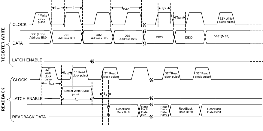 Figure 2. SPI Read-Back Timing Diagram
6.7 Typical Characteristics
VCM = 1.7 V (internal), VinBB = 300 mVrms single-ended sine wave in quadrature, VCC3V = 3.3 V, VCC5V = 5 V, fBB = 4.5 MHz and 5.5 MHz, internal LO, TA = 25°C; FPFD = 1.6 MHz (unless otherwise noted).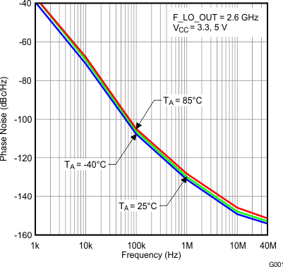 Figure 3. Open-Loop Phase Noise
 vs Frequency and Temperature
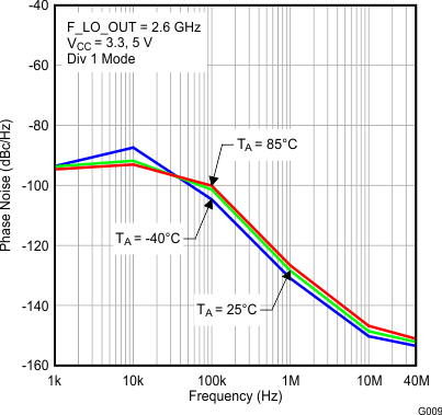
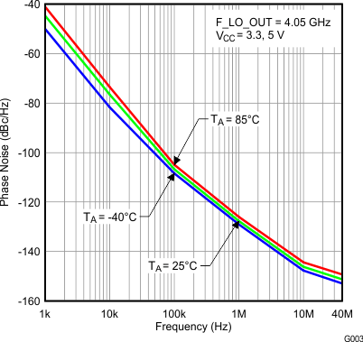 Figure 5. Open Loop Phase Noise
 vs Frequency and Temperature
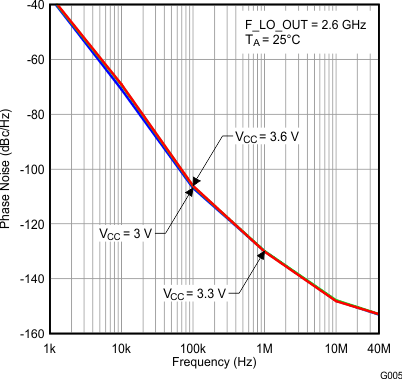 Figure 7. Open Loop Phase Noise
 vs Frequency and Supply Voltage
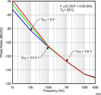 Figure 9. Open Loop Phase Noise
 vs Frequency and Supply Voltage
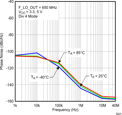 Figure 13. Closed Loop Phase Noise
 vs Frequency and Temperature
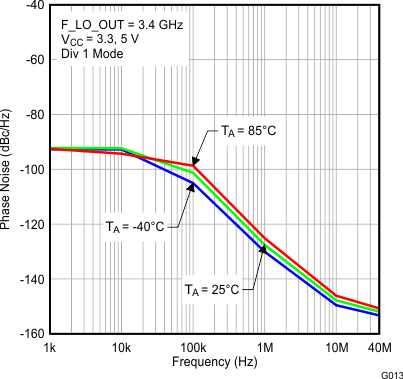 Figure 15. Closed Loop Phase Noise
 vs Frequency and Temperature
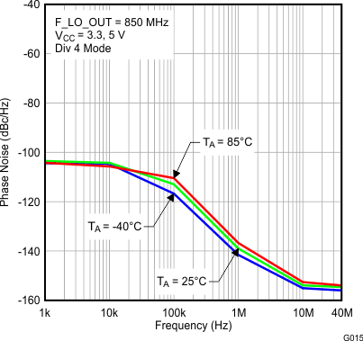 Figure 17. Closed Loop Phase Noise
 vs Frequency and Temperature
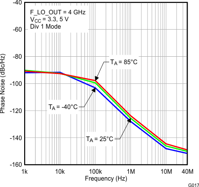 Figure 19. Closed Loop Phase Noise
 vs Frequency and Temperature
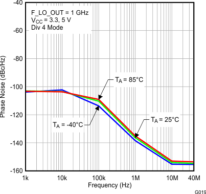 Figure 21. Closed Loop Phase Noise
 vs Frequency and Temperature
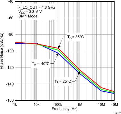 Figure 23. Closed Loop Phase Noise
 vs Frequency and Temperature
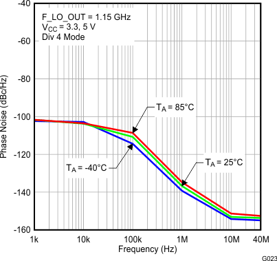 Figure 25. Closed Loop Phase Noise
 vs Frequency and Temperature
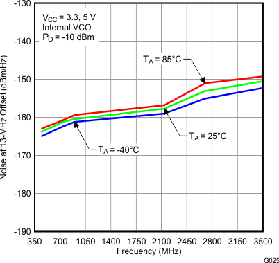 Figure 27. Noise at 13-MHz Offset
 vs Frequency and Temperature With Internal VCO
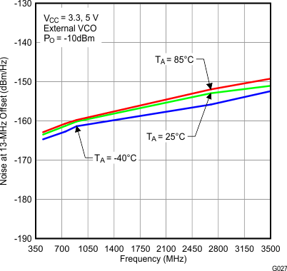 Figure 29. Noise at 13-MHz Offset
 vs Frequency and Temperature With External VCO
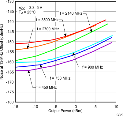 Figure 31. Noise at 13-MHz Offset
 vs Output Power and Frequency
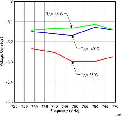 Figure 33. Voltage Gain
 vs Frequency and Temperature at 750 MHz
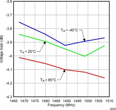 Figure 35. Voltage Gain
 vs Frequency and Temperature at 1500 MHz
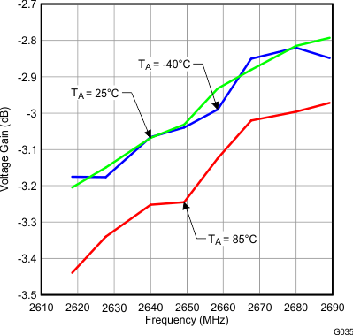 Figure 37. Voltage Gain
 vs Frequency and Temperature at 2650 MHz
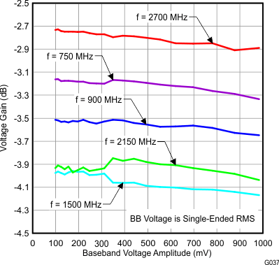 Figure 39. Voltage Gain
 vs Baseband Voltage Amplitude and Frequency
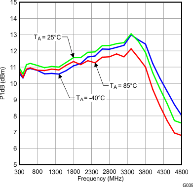 Figure 41. P1dB vs Frequency and Temperature
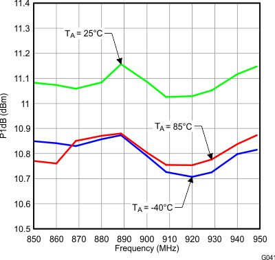 Figure 43. P1dB vs Frequency and Temperature at 900 MHz
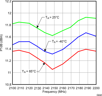 Figure 45. P1dB vs Frequency and Temperature at 2150 MHz
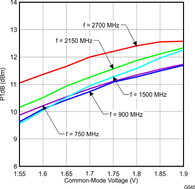 Figure 47. P1dB vs Common-Mode Voltage and Frequency
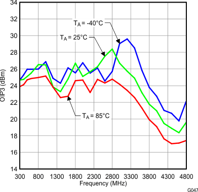 Figure 49. OIP3 vs Frequency and Temperature
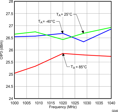 Figure 51. OIP3 vs Frequency and Temperature at 1030 MHz
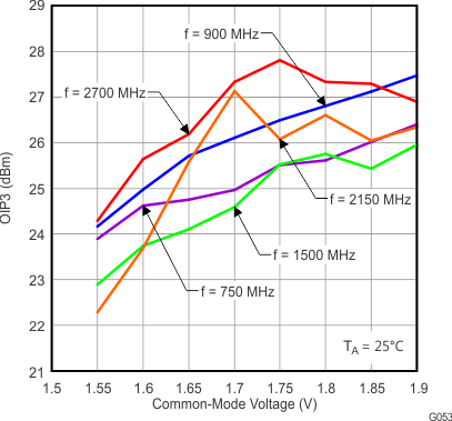
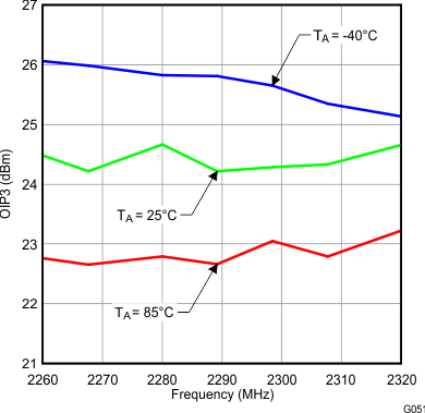 Figure 53. OIP3 vs Frequency and Temperature at 2300 MHz
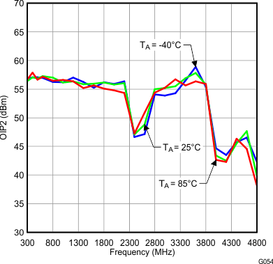 Figure 57. OIP2 vs Frequency and Temperature
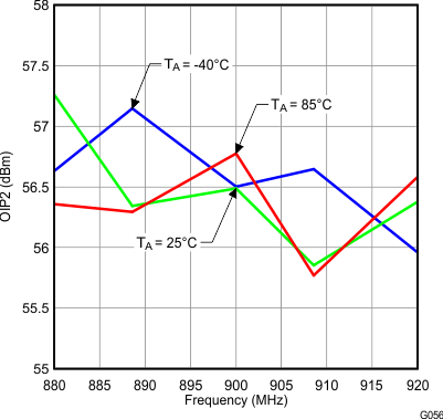 Figure 59. OIP2 vs Frequency and Temperature at 900 MHz
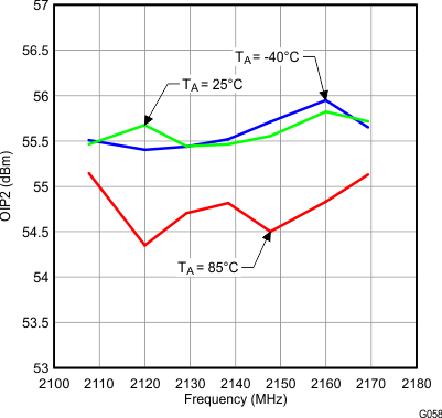 Figure 61. OIP2 vs Frequency and Temperature at 2150 MHz
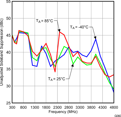 Figure 63. Unadjusted Sideband Suppression
 vs Frequency and Temperature
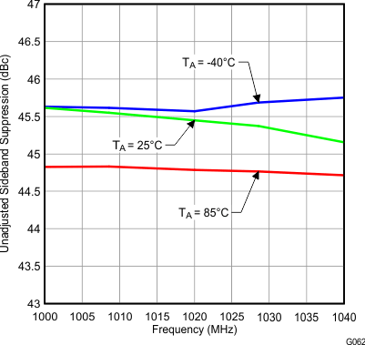 Figure 65. Unadjusted Sideband Suppression
 vs Frequency and Temperature at 1030 MHz
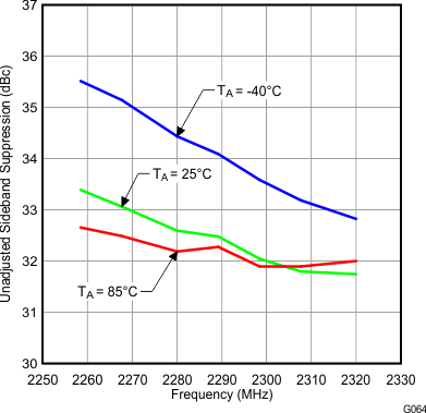 Figure 67. Unadjusted Sideband Suppression
 vs Frequency and Temperature at 2300 MHz
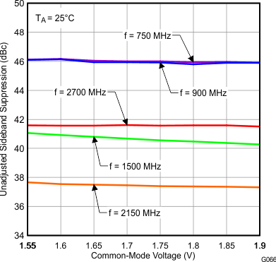 Figure 69. Unadjusted Sideband Suppression
 vs Common-Mode Voltage and Frequency
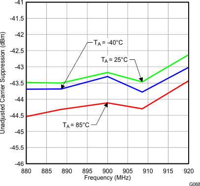 Figure 71. Unadjusted Carrier Suppression
 vs Frequency and Temperature at 900 MHz
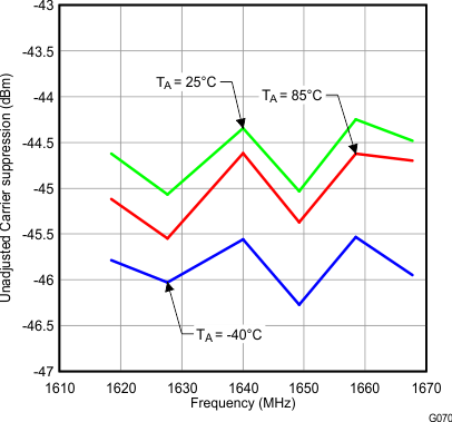 Figure 73. Unadjusted Carrier Suppression
 vs Frequency and Temperature at 1650 MHz
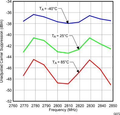 Figure 75. Unadjusted Carrier Suppression
 vs Frequency and Temperature at 2850 MHz
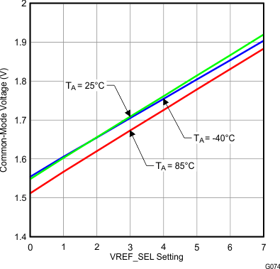 Figure 77. Common-Mode Voltage
 vs VREF_SEL Setting and Temperature
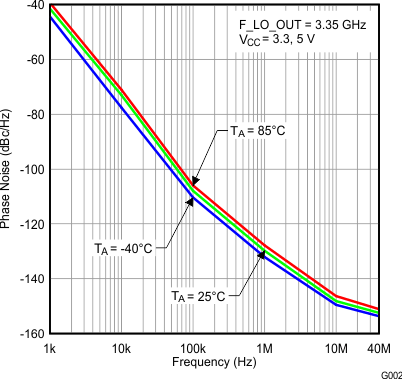 Figure 4. Open Loop Phase Noise
 vs Frequency and Temperature
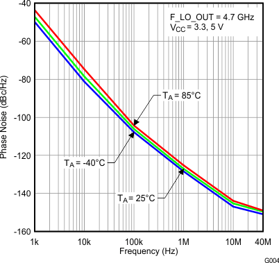 Figure 6. Open Loop Phase Noise
 vs Frequency and Temperature
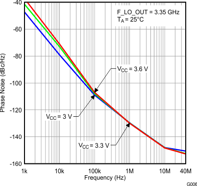 Figure 8. Open Loop Phase Noise
 vs Frequency and Supply Voltage
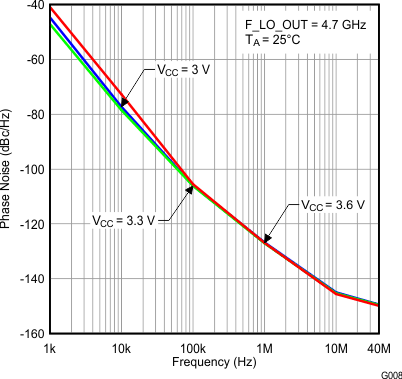 Figure 10. Open Loop Phase Noise
 vs Frequency and Supply Voltage
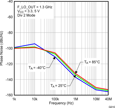 Figure 12. Closed Loop Phase Noise
 vs Frequency and Temperature
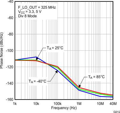 Figure 14. Closed Loop Phase Noise
 vs Frequency and Temperature
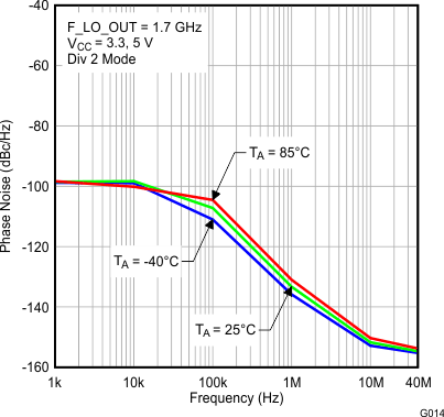 Figure 16. Closed Loop Phase Noise
 vs Frequency and Temperature
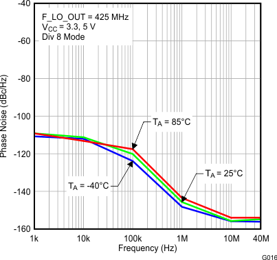 Figure 18. Closed Loop Phase Noise
 vs Frequency and Temperature
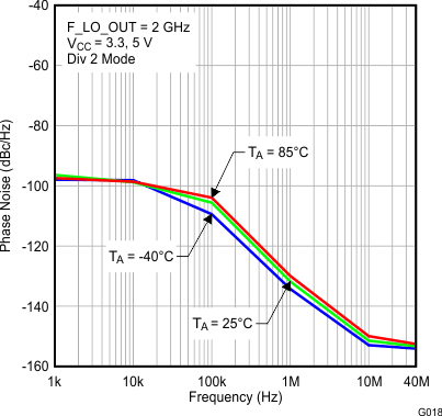 Figure 20. Closed Loop Phase Noise
 vs Frequency and Temperature
 Figure 22. Closed Loop Phase Noise
vs Frequency and Temperature
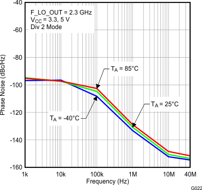 Figure 24. Closed Loop Phase Noise
 vs Frequency and Temperature
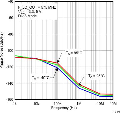 Figure 26. Closed Loop Phase Noise
 vs Frequency and Temperature
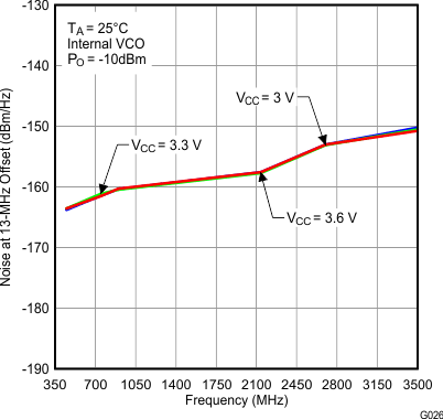 Figure 28. Noise at 13-MHz Offset
 vs Frequency and Supply Voltage With Internal VCO
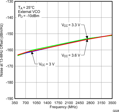 Figure 30. Noise at 13-MHz Offset
 vs Frequency and Supply Voltage With External VCO
 Figure 32. Voltage Gain vs Frequency and Temperature
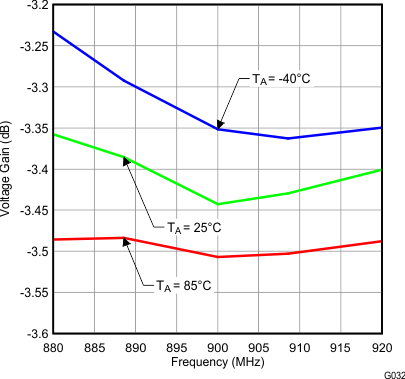 Figure 34. Voltage Gain
 vs Frequency and Temperature at 900 MHz
 Figure 36. Voltage Gain
 vs Frequency and Temperature at 2150 MHz
 Figure 38. Voltage Gain
 vs Common-Mode Voltage and Frequency
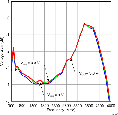 Figure 40. Voltage Gain vs Frequency and Supply Voltage
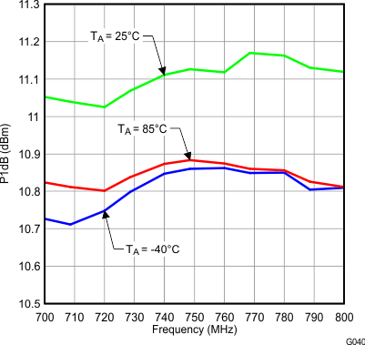 Figure 42. P1dB vs Frequency and Temperature at 750 MHz
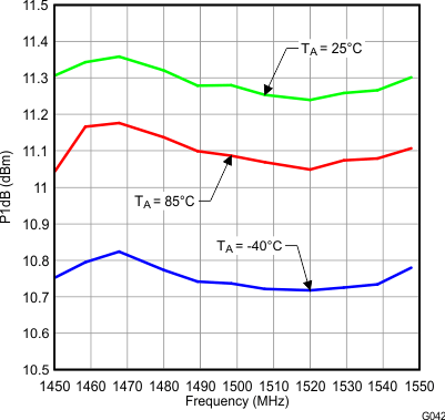 Figure 44. P1dB vs Frequency and Temperature at 1500 MHz
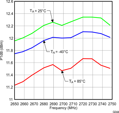 Figure 46. P1dB vs Frequency and Temperature at 2700 MHz
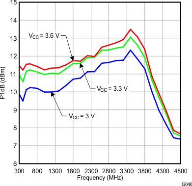 Figure 48. P1dB vs Frequency and Supply Voltage
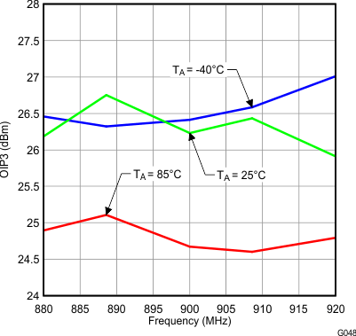 Figure 50. OIP3 vs Temperature and Frequency at 900 MHz
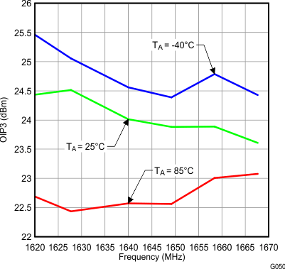 Figure 52. OIP3 vs Frequency and Temperature at 1650 MHz
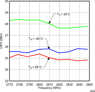 Figure 54. OIP3 vs Frequency and Temperature at 2850 MHz
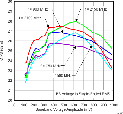 Figure 56. OIP3 vs Baseband Voltage Amplitude and Frequency
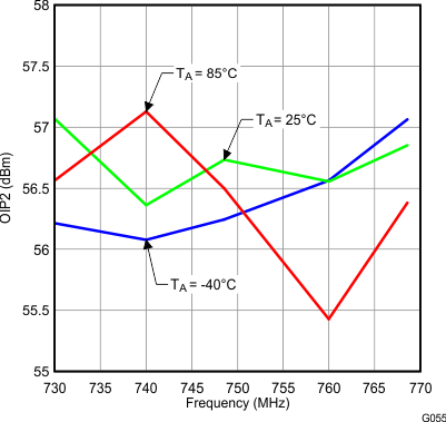 Figure 58. OIP2 vs Frequency and Temperature at 750 MHz
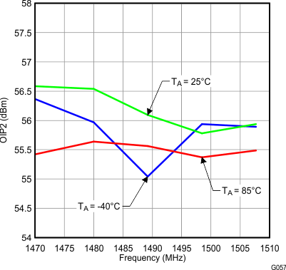 Figure 60. OIP2 vs Frequency and Temperature at 1500 MHz
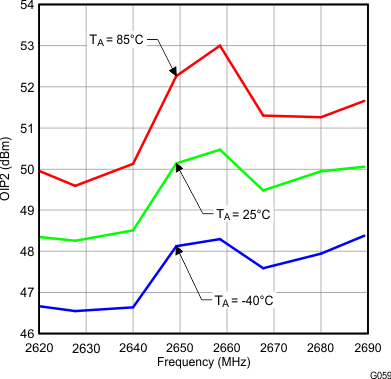 Figure 62. OIP2 vs Frequency and Temperature at 2650 MHz
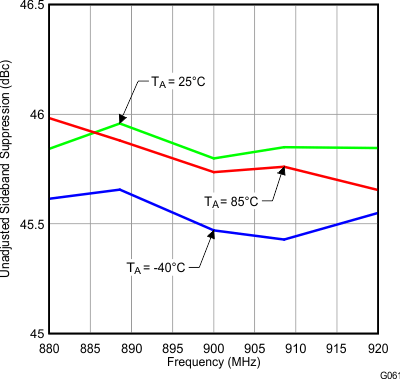 Figure 64. Unadjusted Sideband Suppression
 vs Frequency and Temperature at 900 MHz
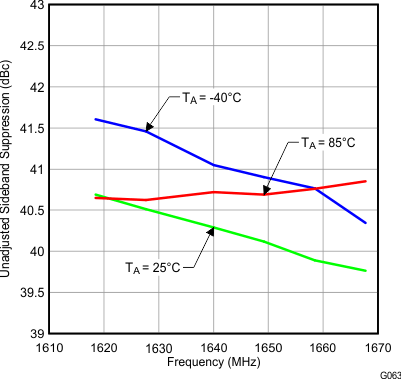 Figure 66. Unadjusted Sideband Suppression
 vs Frequency and Temperature at 1650 MHz
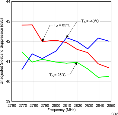 Figure 68. Unadjusted Sideband Suppression
 vs Frequency and Temperature at 2850 MHz
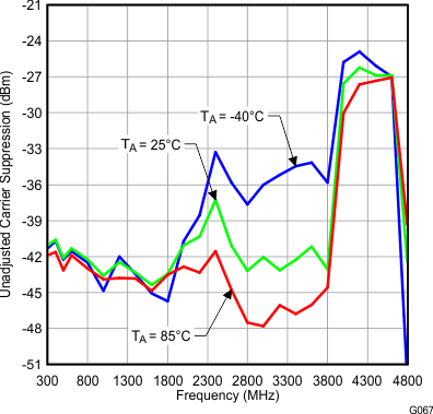 Figure 70. Unadjusted Carrier Suppression
 vs Frequency and Temperature
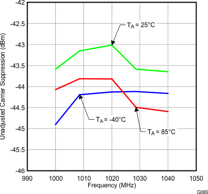 Figure 72. Unadjusted Carrier Suppression
 vs Frequency and Temperature at 1030 MHz
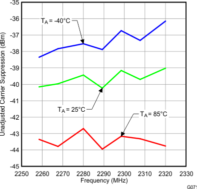 Figure 74. Unadjusted Carrier Suppression
 vs Frequency and Temperature at 2300 MHz
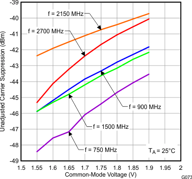 Figure 76. Unadjusted Carrier Suppression
 vs Common-Mode Voltage and Frequency
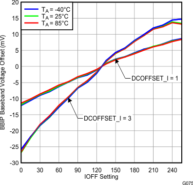 Figure 78. Baseband Voltage Offset
 vs IOFF Setting and Temperature
