ZHCSCN0B May 2014 – February 2017 TRF3722
PRODUCTION DATA.
- 1 特性
- 2 应用
- 3 说明
- 4 修订历史记录
- 5 Pin Configuration and Functions
-
6 Specifications
- 6.1 Absolute Maximum Ratings
- 6.2 ESD Ratings
- 6.3 Recommended Operating Conditions
- 6.4 Thermal Information
- 6.5 Electrical Characteristics
- 6.6 Typical Characteristics
- 6.7 Typical Characteristics - Output Power
- 6.8 Typical Characteristics - Gain
- 6.9 Typical Characteristics - OIP3
- 6.10 Typical Characteristics - OIP2
- 6.11 Typical Characteristics - OP1dB
- 6.12 Typical Characteristics - Noise
- 6.13 Typical Characteristics - Unadjusted CF
- 6.14 Typical Characteristics - Unadjusted SBS
- 6.15 Typical Characteristics - LO Harmonic
- 6.16 Typical Characteristics - BB Harmonic
- 6.17 Typical Characteristics - RF Output Return Loss
- 6.18 Typical Characteristics - PLL/VCO
- 6.19 Typical Characteristics - Current Consumption
- 6.20 Typical Characteristics - Power Dissipation
- 7 Parameter Measurement Information
- 8 Detailed Description
- 9 Application and Implementation
- 10Power Supply Recommendations
- 11Layout
- 12器件和文档支持
- 13机械、封装和可订购信息
9 Application and Implementation
NOTE
Information in the following applications sections is not part of the TI component specification, and TI does not warrant its accuracy or completeness. TI’s customers are responsible for determining suitability of components for their purposes. Customers should validate and test their design implementation to confirm system functionality.
9.1 Application Information
9.2 Typical Application
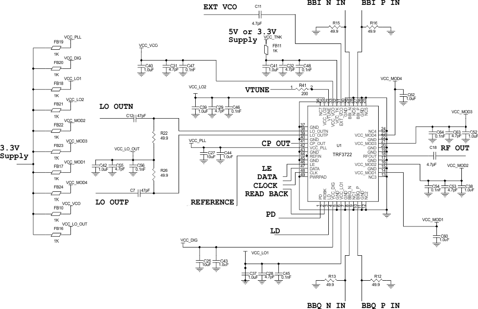
Figure 135 shows a typical application schematic for the TRF3722.
 Figure 135. TRF3722 Application Schematic
9.2.1 Design Requirements
Table 17 lists the pin termination requirements and interfacing for the circuit.
Table 17. Termination Requirements and Interfacing
| PIN | NAME | DESCRIPTION |
|---|---|---|
| 47 | DATA | 4WI data input: digital input, high impedance |
| 2 | RDBK | Readback output; digital output pins can source or sink up to 8 mA of current |
| 3 | LD | Lock detector digital output, as configured by MUX_CTRL |
| 8,10,27,29 | BBI_P, BBI_N, BBQ_P, BBQ_N | In-phase and quadrature baseband differential baseband signals. Typical 0.25V common mode is needed |
| 18 | RFOUT | Modulator RF output: must be ac-coupled and can drive 50 Ω load |
| 31 | EXT_VCO | External local oscillator input: high impedance, normally ac-coupled. If unused terminate to 50 ohms load |
| 38,39 | LO_OUTP, LO_OUTN | Local oscillator output: open-collector output. A pull-up resistor is LO_OUT required, normally ac-coupled. |
| 44 | REFIN | Reference clock input: high impedance, normally ac-coupled |
| 46 | LE | Serial interface latch enable: digital input, high impedance |
| 48 | CLK | Serial interface clock input: digital input, high impedance |
| 47 | DATA | Serial interface data input: digital input, high impedance |
9.2.2 Detailed Design Procedures: DAC to Modulator Interface Network
Digital-to-analog converter (DAC) can interface directly with the TRF3722 modulator. The common-mode voltage of the DAC and the modulator baseband inputs should be properly maintained. With the proper interface network, the common-mode voltage of the DAC can be translated to the proper common-mode voltage of the modulator. The TRF3722 common-mode voltage is typically 0.25 V, and is ideally suited to interface with the DAC3482/3484 (DAC348x) and DAC38J8x family. The interface network is shown in Figure 136.
 Figure 136. DAC348x Interface with the TRF3722 Modulator
The DAC348x requires a load resistance of 25 Ω per branch to maintain its optimum voltage swing of 1-VPP differential with a 20-mA max current setting. The load of the DAC is separated into two parallel 50-Ω resistors placed on the input and output side of the low-pass filter. This configuration provides the proper resistive load to the DAC while also providing a convenient 50-Ω source and load termination for the filter.
9.2.3 Application Curves: DAC34H84 with TRF3722 Modulator Performance
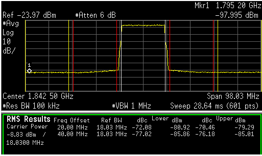
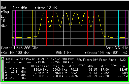
The cascaded combination of the DAC34H84 and TRF3722 modulator yields excellent system parameters suitable for high-performance applications. Figure 137 and Figure 138 show 152.9 MHz IF adjacent channel power ratio (ACPR) performance.
- Mode integer
- PFD: 3.2 MHz
- Reference: 153.6 MHz
- LO = 1689.6 MHz
- IF = 152.9 MHz
- RF= 1842.5 MHz

 Figure 138. 152.9 MHz IF, 6 Carrier MC-GSM DAC34H84 + TRF3722 ACPR Performance