ZHCSD77A May 2014 – December 2014 TRF37A32 , TRF37B32 , TRF37C32
PRODUCTION DATA.
- 1 特性
- 2 应用
- 3 说明
- 4 简化电路原理图
- 5 修订历史记录
- 6 Pin Configuration and Functions
-
7 Specifications
- 7.1 Absolute Maximum Ratings
- 7.2 ESD Ratings
- 7.3 Recommended Operating Conditions
- 7.4 Thermal Information
- 7.5 Electrical Characteristics, TRF37A32
- 7.6 Electrical Characteristics, TRF37B32
- 7.7 Electrical Characteristics, TRF37C32
- 7.8 Timing Requirements
- 7.9 Typical Characteristics (TRF37A32)
- 7.10 Typical Characteristics (TRF37B32)
- 7.11 Typical Characteristics (TRF37C32)
- 8 Detailed Description
- 9 Applications and Implementation
- 10Power Supply Recommendations
- 11Layout
- 12器件和文档支持
- 13机械、封装和可订购信息
9 Applications and Implementation
NOTE
Information in the following applications sections is not part of the TI component specification, and TI does not warrant its accuracy or completeness. TI’s customers are responsible for determining suitability of components for their purposes. Customers should validate and test their design implementation to confirm system functionality.
9.1 Application Information
The devices are high-linearity, wideband receive mixers. They are typically implemented to convert frequencies from the range 400 MHz to 3800 MHz into the range 30 MHz to 600 MHz.
9.2 Typical Application
The TRF37x32 device is typically placed in a system as illustrated in Figure 75.
 Figure 75. Typical System Implementation of TRF37x32
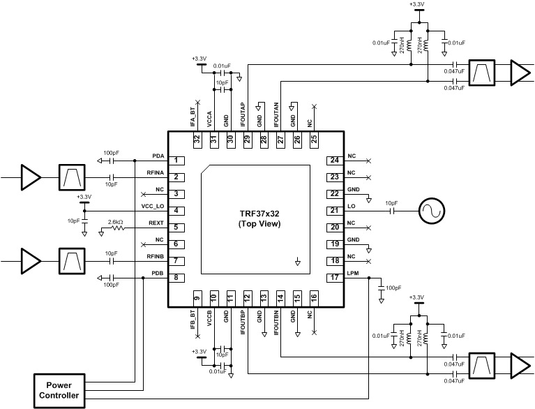
A typical schematic for the TRF37x32 is shown in Figure 76.
 Figure 76. Typical Application Schematic for TRF37x32
9.2.1 Design Requirements
For this design example, use the parameters shown in Table 3.
Table 3. Design Parameters
| MIXER PARAMETER | EXAMPLE APPLICATION REQUIREMENTS(1) | TRF37B32 PERFORMANCE (TYPICAL) |
|---|---|---|
| RF Frequency Range | 2300 - 2400 MHz | 700 - 2700 MHz |
| IF Frequency Range | 318.64 - 418.64 MHz | 30 - 600 MHz |
| Gain | 9 - 10 dB | 9.7 dB at FRF = 2300 MHz |
| NF | < 12 dB | 10 dB at FRF = 2300 MHz |
| IIP3 | > 28 dBm | 30 dBm at FRF = 2300 MHz |
| IP1dB | > 8 dBm | 11 dBm at FRF = 2300 MHz |
9.2.2 Detailed Design Procedure
9.2.2.1 Power Level
Input power should back off from the TRF37x32 compression point for linear operation, ideally by 10dB or more. Choose LNA gain and gain scheduling in order to set the appropriate power level at the RF input to the TRF37x32.
Given the expected input power level, use the expected gain through the mixer and other elements, such as SAW filter and matching networks, to calculate the voltage expected at the ADC. Adjust gain and loss elements to maximize the utilization of ADC dynamic range.
9.2.2.2 Matching
Although the TRF37x32 was designed to interface with 50 Ω RF and LO and 200 Ω differential signal lines, some elements in the signal chain may not present a wideband real impedance. Matching components are optional but may be used at these ports to improve impedance alignment, thereby increasing power delivered to the RF node and decreasing reflected and radiated power. Good matching maximizes isolation and linearity performance.
9.2.2.3 RF Input Component Selection
The blocking capacitor value on the RF input should be selected according to Table 1.
9.2.2.4 IF Output Component Selection
Use high Q inductors for pull-up biasing on the IF output. 270 nH 0805-size wirewound indictors provides excellent linearity and gain. Larger inductor values may compress the IF bandwidth, while smaller package sizes tend to introduce lower inductor Q ratings.
Connect the supply nodes of both inductors for a given channel symmetrically to the VCC net with close proximity to ensure balanced connection to the supply.
9.2.2.5 Frequency Planning
The LO and RF inputs are both designed for wideband behavior, and either high-side or low-side injection may be used interchangeably across most of the RF band. At the extreme RF frequencies the LO input bandwidth will force operation to either high side injection (HSI) or low side injection (LSI). Table 2 provides the operating range of the LO for each device. Where possible it is recommended to utilize low side injection to keep the power dissipation to a minimum.
9.2.2.6 Control Terminal Transients
Decoupling capacitors reduce terminal noise but also slow transient response. Adjust external capacitors in order to meet specified power-on and power-off response times. Apply transmission line matching techniques to achieve the fastest response times.
9.2.3 Application Curves
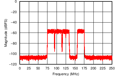
 Figure 77. 4-Carrier Receiver Application