ZHCSD77A May 2014 – December 2014 TRF37A32 , TRF37B32 , TRF37C32
PRODUCTION DATA.
- 1 特性
- 2 应用
- 3 说明
- 4 简化电路原理图
- 5 修订历史记录
- 6 Pin Configuration and Functions
-
7 Specifications
- 7.1 Absolute Maximum Ratings
- 7.2 ESD Ratings
- 7.3 Recommended Operating Conditions
- 7.4 Thermal Information
- 7.5 Electrical Characteristics, TRF37A32
- 7.6 Electrical Characteristics, TRF37B32
- 7.7 Electrical Characteristics, TRF37C32
- 7.8 Timing Requirements
- 7.9 Typical Characteristics (TRF37A32)
- 7.10 Typical Characteristics (TRF37B32)
- 7.11 Typical Characteristics (TRF37C32)
- 8 Detailed Description
- 9 Applications and Implementation
- 10Power Supply Recommendations
- 11Layout
- 12器件和文档支持
- 13机械、封装和可订购信息
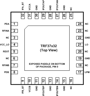
6 Pin Configuration and Functions
RTV PACKAGE
(TOP VIEW)

Pin Functions
| PIN | I/O | DESCRIPTION | |
|---|---|---|---|
| NAME | NO. | ||
| PDA | 1 | Digital Input | Power down for channel A (1 = PD; 0 or open = powered) |
| RFINA | 2 | Analog Input | RF input for channel A |
| NC | 3 | N/A | No connect |
| VCC_LO | 4 | Supply | VCC supply for the LO circuitry |
| REXT | 5 | Bias | External bias resistor |
| NC | 6 | N/A | No connect |
| RFINB | 7 | Analog Input | RF input for channel B |
| PDB | 8 | Digital Input | Power down for channel B (1 = PD; 0 or open = powered) |
| IFB_BT | 9 | N/A | IF channel B bias control; leave unconnected |
| VCCB | 10 | Supply | Power supply for channel B |
| GND | 11 | Ground | Ground |
| IFOUTBP | 12 | Analog Output | IF out channel B: positive |
| GND | 13 | Ground | Ground |
| IFOUTBN | 14 | Analog Output | IF out channel B: negative |
| GND | 15 | Ground | Ground |
| NC | 16 | N/A | No connect |
| LPM | 17 | Digital Input | Low power mode (0 = normal; 1 = low power) |
| NC | 18 | N/A | No connect |
| GND | 19 | Ground | Ground |
| NC | 20 | N/A | No connect |
| LO | 21 | Analog Input | Local oscillator (LO) input |
| GND | 22 | Ground | Ground |
| NC | 23 | N/A | No connect |
| NC | 24 | N/A | No connect |
| NC | 25 | N/A | No connect |
| GND | 26 | Ground | Ground |
| IFOUTAN | 27 | Analog Output | IF out channel A: negative |
| GND | 28 | Ground | Ground |
| IFOUTAP | 29 | Analog Output | IF out channel A: positive |
| GND | 30 | Ground | Ground |
| VCCA | 31 | Supply | Power supply for channel A |
| IFA_BT | 32 | N/A | IF channel A bias control; leave unconnected |