ZHCSCH8 May 2014 TRF37C73
PRODUCTION DATA.
7 Detailed Description
7.1 Overview
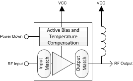
The device is a 3.3 V general purpose RF gain block. It is a SiGe Darlington amplifier with integrated 50 Ω input and output matching. The device contains an active bias circuit to maintain performance over a wide temperature and voltage range. The included power down function allows the amplifier to shut down saving power when the amplifier is not needed. Fast shut down and start up enable the amplifier to be used in a host of time division duplex applications.
7.2 Functional Block Diagram

7.3 Feature Description
The TRF37C73 is a fixed gain RF amplifier. It is internally matched to 50 Ω on both the input and output. It is a fully cascadable general purpose amplifier. The included active bias circuitry ensures the amplifier performance is optimized over the full operating temperature and voltage ranges.
7.4 Device Functional Modes
7.4.1 Power Down
The TRF37C73 PWDN pin can be left unconnected for normal operation or a logic-high for disable mode operation. For applications that use the power down mode, normal 5 V TLL levels are supported.