ZHCS266F June 2011 – May 2017 TRF7960A
PRODUCTION DATA.
- 1器件概述
- 2修订历史记录
- 3Device Characteristics
- 4Terminal Configuration and Functions
- 5Specifications
-
6Detailed Description
- 6.1 Functional Block Diagram
- 6.2 Power Supplies
- 6.3 Supply Arrangements
- 6.4 Supply Regulator Settings
- 6.5 Power Modes
- 6.6 Receiver – Analog Section
- 6.7 Receiver – Digital Section
- 6.8 Oscillator Section
- 6.9 Transmitter - Analog Section
- 6.10 Transmitter - Digital Section
- 6.11 Transmitter – External Power Amplifier or Subcarrier Detector
- 6.12 Communication Interface
- 6.13
Direct Commands from MCU to Reader
- 6.13.1 Command Codes
- 6.13.2 Reset FIFO (0x0F)
- 6.13.3 Transmission With CRC (0x11)
- 6.13.4 Transmission Without CRC (0x10)
- 6.13.5 Delayed Transmission With CRC (0x13)
- 6.13.6 Delayed Transmission Without CRC (0x12)
- 6.13.7 Transmit Next Time Slot (0x14)
- 6.13.8 Block Receiver (0x16)
- 6.13.9 Enable Receiver (0x17)
- 6.13.10 Test Internal RF (RSSI at RX Input With TX On) (0x18)
- 6.13.11 Test External RF (RSSI at RX Input With TX Off) (0x19)
- 6.13.12 Register Preset
- 6.14
Register Description
- 6.14.1
Register Overview
- 6.14.1.1 Main Configuration Registers
- 6.14.1.2
Protocol Subsetting Registers
- 6.14.1.2.1 ISO14443B TX Options Register (0x02)
- 6.14.1.2.2 ISO14443A High-Bit-Rate and Parity Options Register (0x03)
- 6.14.1.2.3 TX Timer High Byte Control Register (0x04)
- 6.14.1.2.4 TX Timer Low Byte Control Register (0x05)
- 6.14.1.2.5 TX Pulse Length Control Register (0x06)
- 6.14.1.2.6 RX No Response Wait Time Register (0x07)
- 6.14.1.2.7 RX Wait Time Register (0x08)
- 6.14.1.2.8 Modulator and SYS_CLK Control Register (0x09)
- 6.14.1.2.9 RX Special Setting Register (0x0A)
- 6.14.1.2.10 Regulator and I/O Control Register (0x0B)
- 6.14.1.3 Status Registers
- 6.14.1.4 Test Registers
- 6.14.1.5 FIFO Control Registers
- 6.14.1
Register Overview
- 7Applications, Implementation, and Layout
- 8器件和文档支持
- 9机械、封装和可订购信息
6.8 Oscillator Section
The 13.56-MHz oscillator is controlled by the Chip Status Control register (0x00) and the EN and EN2 signals. The oscillator generates the RF frequency for the RF output stage and the clock source for the digital section. The buffered clock signal is available at pin 27 (SYS_CLK) for external circuits. B4 and B5 inside the Modulation and SYS_CLK register (0x09) can be used to divide the external SYS_CLK signal at pin 27 by 1, 2, or 4.
Typical start-up time from complete power down is in the range of 3.5 ms.
During Power Down Mode 2 (EN = 0, EN2 = 1) the frequency of SYS_CLK is switched to 60 kHz (typical).
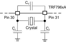
The 13.56-MHz crystal must be connected between pin 30 and pin 31. The external shunt capacitors values for C1 and C2 must be calculated based on the specified load capacitance of the crystal being used. The external shunt capacitors are calculated as two identical capacitors in series plus the stray capacitance of the TRF7960A and parasitic PCB capacitance in parallel to the crystal.
The parasitic capacitance (CS , stray and parasitic PCB capacitance) can be estimated at 4 to 5 pF (typical).
As an example, using a crystal with a required load capacitance (CL) of 18 pF, the calculation is as follows (see Figure 6-4):
C1= C2 = 2 × (CL – CS) = 2 × (18 pF – 4.5 pF) = 27 pF
Place a 27-pF capacitor on pins 30 and 31 to ensure proper crystal oscillator operation.
Table 6-5 shows the minimum characteristics recommended for any crystal used with TRF7960A.
Table 6-5 Minimum Crystal Recommendations
| PARAMETER | SPECIFICATION |
|---|---|
| Frequency | 13.56 MHz |
| Mode of operation | Fundamental |
| Type of resonance | Parallel |
| Frequency tolerance | ±20 ppm |
| Aging | <5 ppm/year |
| Operation temperature range | –40°C to 85°C |
As an alternative, an external clock oscillator source can be connected to pin 31 to provide the system clock, and pin 30 can be left open.
