ZHCS266F June 2011 – May 2017 TRF7960A
PRODUCTION DATA.
- 1器件概述
- 2修订历史记录
- 3Device Characteristics
- 4Terminal Configuration and Functions
- 5Specifications
-
6Detailed Description
- 6.1 Functional Block Diagram
- 6.2 Power Supplies
- 6.3 Supply Arrangements
- 6.4 Supply Regulator Settings
- 6.5 Power Modes
- 6.6 Receiver – Analog Section
- 6.7 Receiver – Digital Section
- 6.8 Oscillator Section
- 6.9 Transmitter - Analog Section
- 6.10 Transmitter - Digital Section
- 6.11 Transmitter – External Power Amplifier or Subcarrier Detector
- 6.12 Communication Interface
- 6.13
Direct Commands from MCU to Reader
- 6.13.1 Command Codes
- 6.13.2 Reset FIFO (0x0F)
- 6.13.3 Transmission With CRC (0x11)
- 6.13.4 Transmission Without CRC (0x10)
- 6.13.5 Delayed Transmission With CRC (0x13)
- 6.13.6 Delayed Transmission Without CRC (0x12)
- 6.13.7 Transmit Next Time Slot (0x14)
- 6.13.8 Block Receiver (0x16)
- 6.13.9 Enable Receiver (0x17)
- 6.13.10 Test Internal RF (RSSI at RX Input With TX On) (0x18)
- 6.13.11 Test External RF (RSSI at RX Input With TX Off) (0x19)
- 6.13.12 Register Preset
- 6.14
Register Description
- 6.14.1
Register Overview
- 6.14.1.1 Main Configuration Registers
- 6.14.1.2
Protocol Subsetting Registers
- 6.14.1.2.1 ISO14443B TX Options Register (0x02)
- 6.14.1.2.2 ISO14443A High-Bit-Rate and Parity Options Register (0x03)
- 6.14.1.2.3 TX Timer High Byte Control Register (0x04)
- 6.14.1.2.4 TX Timer Low Byte Control Register (0x05)
- 6.14.1.2.5 TX Pulse Length Control Register (0x06)
- 6.14.1.2.6 RX No Response Wait Time Register (0x07)
- 6.14.1.2.7 RX Wait Time Register (0x08)
- 6.14.1.2.8 Modulator and SYS_CLK Control Register (0x09)
- 6.14.1.2.9 RX Special Setting Register (0x0A)
- 6.14.1.2.10 Regulator and I/O Control Register (0x0B)
- 6.14.1.3 Status Registers
- 6.14.1.4 Test Registers
- 6.14.1.5 FIFO Control Registers
- 6.14.1
Register Overview
- 7Applications, Implementation, and Layout
- 8器件和文档支持
- 9机械、封装和可订购信息
6.12.6 Serial Interface Communication (SPI)
When an SPI interface is used, I/O pins I/O_2, I/O_1, and I/O_0 must be hard-wired as specified in Table 6-6. On power up, the TRF7960A looks for the status of these pins; if they are not the same (not all high, or not all low), the reader enters into one of two possible SPI modes:
- SPI with slave select
- SPI without slave select
or
The choice of one of these modes over the other should be made based on the available GPIOs and the desired control of the system.
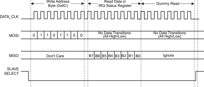
The serial communications work in the same manner as the parallel communications with respect to the FIFO, except for the following condition. On receiving an IRQ from the reader, the MCU reads the TRF7960A IRQ Status register to determine how to service the reader. After this, the MCU must to do a dummy read to clear the reader's IRQ Status register. The dummy read is required in SPI mode, because the reader's IRQ Status register needs an additional clock cycle to clear the register. This is not required in parallel mode, because the additional clock cycle is included in the Stop condition.
A procedure for a dummy read is as follows:
- Starting the dummy read
- When using slave select (SS): set SS bit low
- When not using SS: start condition is when SCLK is high
- Send address word to IRQ Status register (0x0C) with read and continuous address mode bits set to 1
- Read 1 byte (8 bits) from IRQ Status register (0x0C)
- Dummy read 1 byte from register 0Dh (collision position and interrupt mask)
- Stopping the dummy read
- When using slave select (SS): set SS bit high
- When not using SS: stop condition when SCLK is high
 Figure 6-14 Procedure for Dummy Read
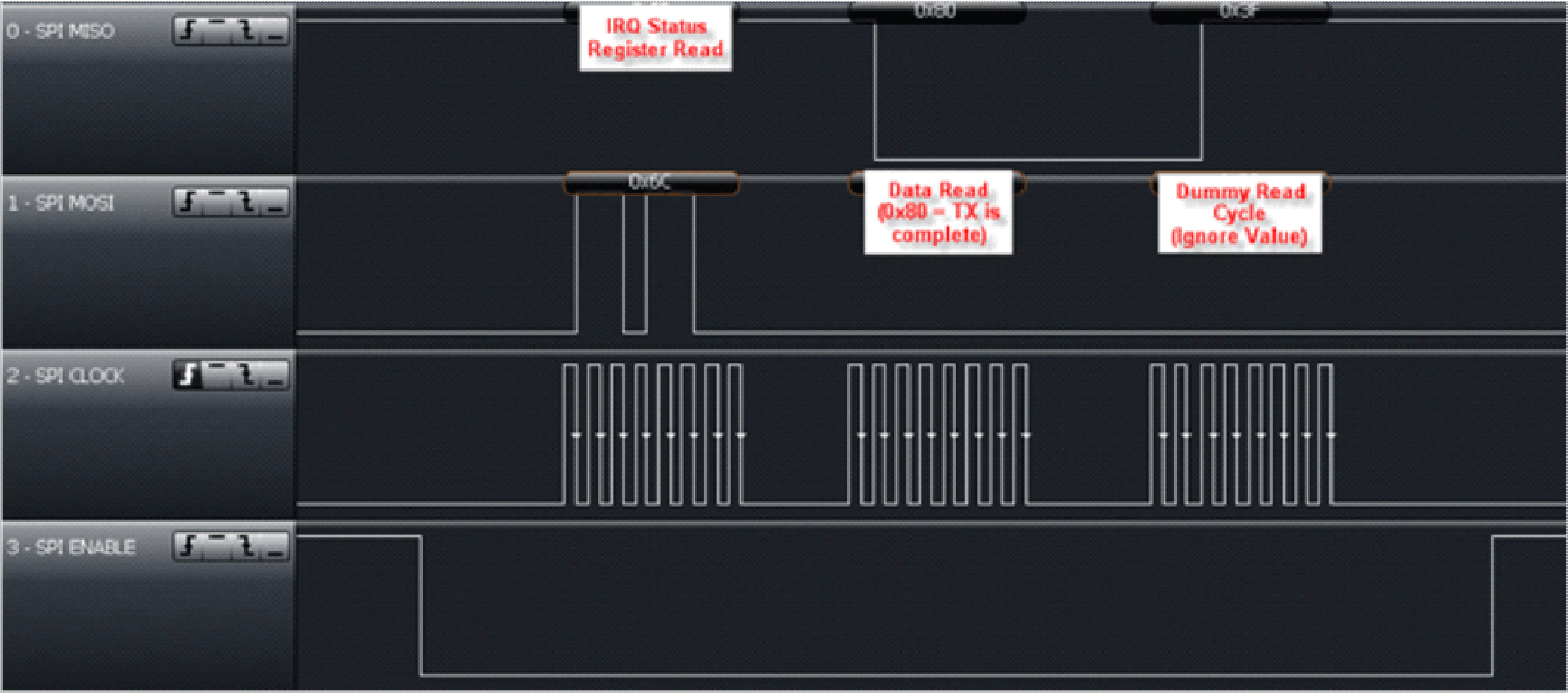
 Figure 6-15 Dummy Read Using SPI With SS