ZHCS266F June 2011 – May 2017 TRF7960A
PRODUCTION DATA.
- 1器件概述
- 2修订历史记录
- 3Device Characteristics
- 4Terminal Configuration and Functions
- 5Specifications
-
6Detailed Description
- 6.1 Functional Block Diagram
- 6.2 Power Supplies
- 6.3 Supply Arrangements
- 6.4 Supply Regulator Settings
- 6.5 Power Modes
- 6.6 Receiver – Analog Section
- 6.7 Receiver – Digital Section
- 6.8 Oscillator Section
- 6.9 Transmitter - Analog Section
- 6.10 Transmitter - Digital Section
- 6.11 Transmitter – External Power Amplifier or Subcarrier Detector
- 6.12 Communication Interface
- 6.13
Direct Commands from MCU to Reader
- 6.13.1 Command Codes
- 6.13.2 Reset FIFO (0x0F)
- 6.13.3 Transmission With CRC (0x11)
- 6.13.4 Transmission Without CRC (0x10)
- 6.13.5 Delayed Transmission With CRC (0x13)
- 6.13.6 Delayed Transmission Without CRC (0x12)
- 6.13.7 Transmit Next Time Slot (0x14)
- 6.13.8 Block Receiver (0x16)
- 6.13.9 Enable Receiver (0x17)
- 6.13.10 Test Internal RF (RSSI at RX Input With TX On) (0x18)
- 6.13.11 Test External RF (RSSI at RX Input With TX Off) (0x19)
- 6.13.12 Register Preset
- 6.14
Register Description
- 6.14.1
Register Overview
- 6.14.1.1 Main Configuration Registers
- 6.14.1.2
Protocol Subsetting Registers
- 6.14.1.2.1 ISO14443B TX Options Register (0x02)
- 6.14.1.2.2 ISO14443A High-Bit-Rate and Parity Options Register (0x03)
- 6.14.1.2.3 TX Timer High Byte Control Register (0x04)
- 6.14.1.2.4 TX Timer Low Byte Control Register (0x05)
- 6.14.1.2.5 TX Pulse Length Control Register (0x06)
- 6.14.1.2.6 RX No Response Wait Time Register (0x07)
- 6.14.1.2.7 RX Wait Time Register (0x08)
- 6.14.1.2.8 Modulator and SYS_CLK Control Register (0x09)
- 6.14.1.2.9 RX Special Setting Register (0x0A)
- 6.14.1.2.10 Regulator and I/O Control Register (0x0B)
- 6.14.1.3 Status Registers
- 6.14.1.4 Test Registers
- 6.14.1.5 FIFO Control Registers
- 6.14.1
Register Overview
- 7Applications, Implementation, and Layout
- 8器件和文档支持
- 9机械、封装和可订购信息
6.12.6.2 Serial Interface Mode With Slave Select (SS)
The serial interface is in reset while the Slave Select signal is high. Serial data in (MOSI) changes on the falling edge and is validated in the reader on the rising edge (see Figure 6-17). Communication is terminated when the Slave Select signal goes high.
All words must be 8 bits long with the MSB transmitted first.
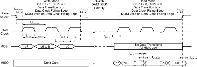 Figure 6-17 SPI With Slave Select Timing
The read command is sent out on the MOSI pin, MSB first, in the first eight clock cycles. MOSI data changes on the falling edge, and is validated in the reader on the rising edge, as shown in Figure 6-17. During the write cycle, the serial data out (MISO) is not valid. After the last read command bit (B0) is validated at the eighth rising edge of SCLK, after half a clock cycle, valid data can be read on the MISO pin at the falling edge of SCLK. It takes eight clock edges to read out the full byte (MSB first).
When using the hardware SPI (for example, an MSP430 hardware SPI) to implement this feature, care must be taken to switch the SCLK polarity after write phase for proper read operation. The example clock polarity for the Figure 6-17 shows the MSP430-specific environment in the write-mode and read-mode boxes. See the USART-SPI chapter for any specific microcontroller family for further information on the setting the appropriate clock polarity. This clock polarity switch must be done for all read (single or continuous) operations. The MOSI (serial data out) should not have any transitions (all high or all low) during the read cycle. The Slave Select should be low during the whole write and read operation.
See Section 5.6, Switching Characteristics, for the timing values shown in Figure 6-17.
Figure 6-18 shows the continuous read operation.
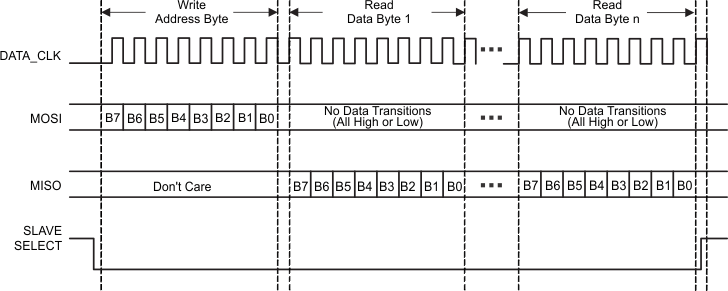 Figure 6-18 Continuous Read Operation Using SPI With Slave Select
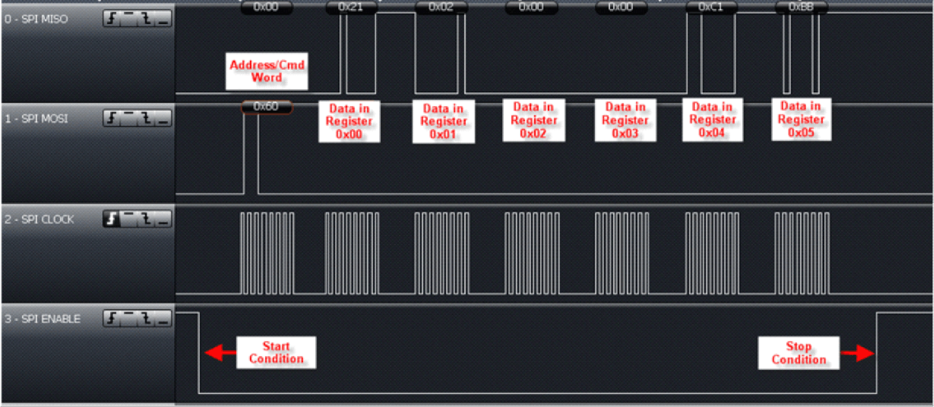 Figure 6-19 Continuous Read of Registers 0x00 to 0x05 Using SPI With SS
Figure 6-20 shows performing a Single Slot Inventory Command as an example. Reader registers (in this example) are configured for 5-VDC input and default operation. Full sequences for other settings and protocols can be downloaded from http://www.ti.com/lit/zip/sloc240.
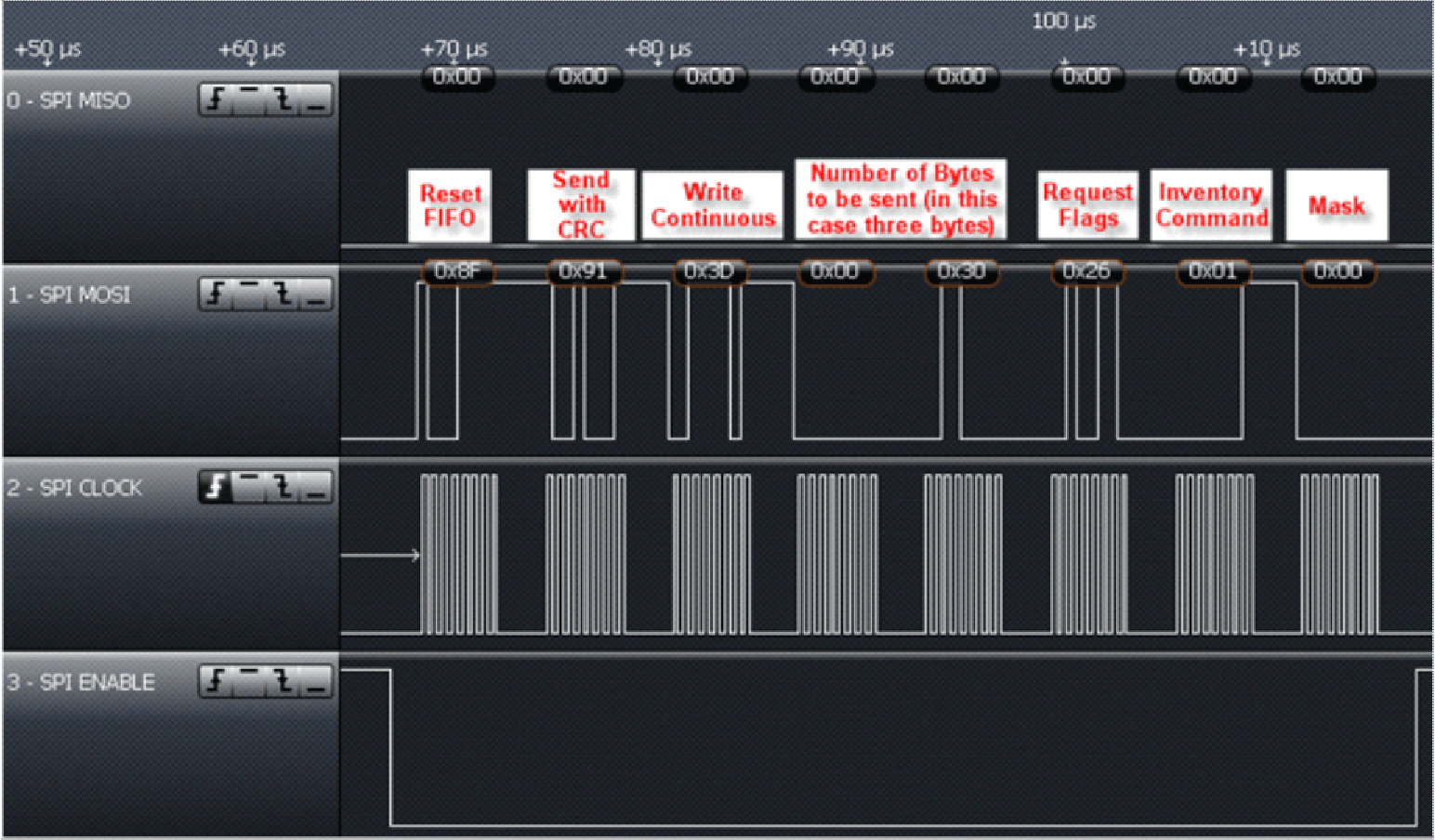 Figure 6-20 Inventory Command Sent From MCU to TRF7960A
 The TRF7960A reads these bytes from the MCU and then sends out Request Flags, Inventory Command, and Mask over the air to the ISO/IEC 15693 transponder. After these three bytes have been transmitted, an interrupt occurs from the reader to indicate back to the MCU that the transmission has been completed. In the example shown in Figure 6-21, this IRQ occurs approximately 1.6 ms after the SS line goes high after the Inventory command is sent out.
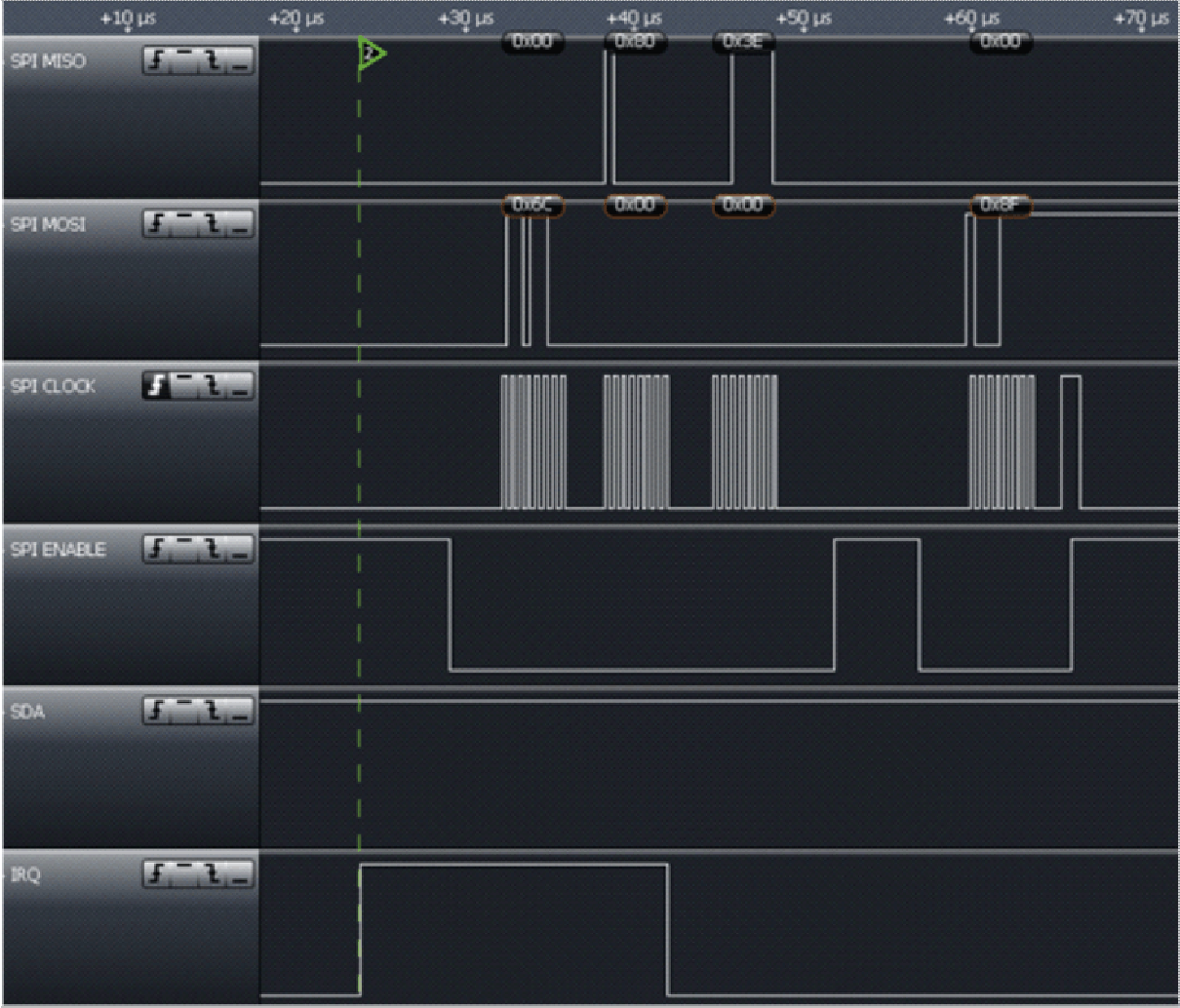 Figure 6-21 IRQ After Inventory Command
The IRQ Status register read (0x6C) yields 0x80, which indicates that TX is complete. This is followed by dummy clock and reset of FIFO with dummy clock. Then, if a tag is in the field and no error is detected by the reader, a second interrupt is expected and occurs (in this example) approximately 4 ms after first IRQ is read and cleared.
In the continuation of the example (see Figure 6-22), the IRQ Status register is read using method previously recommended, followed by a single read of the FIFO Status register, which indicates that there are at least 9 bytes to be read out.
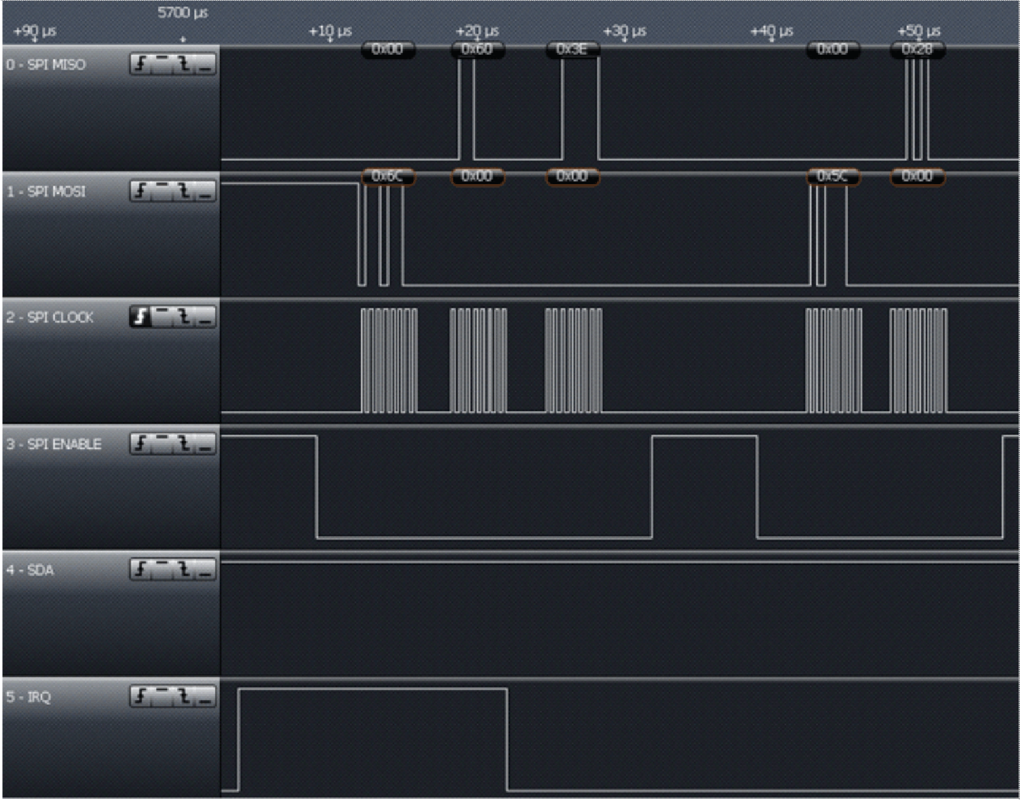 Figure 6-22 IRQ Status Register Read Followed by FIFO Status Register Read
This is followed by a continuous read of the FIFO (see Figure 6-23). The first byte is 0x00 for no error. The next byte is the DSFID (usually shipped by manufacturer as 0x00), then the UID, shown here up to the next most significant byte (MSByte), the MFG code (0x07 to indicate TI silicon).
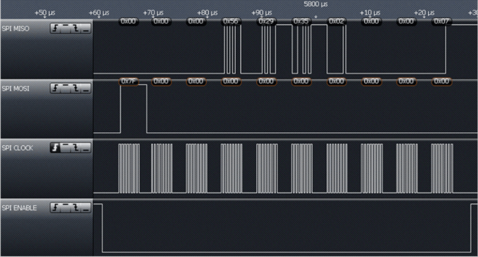 Figure 6-23 Continuous Read of FIFO
This is followed by another IRQ approximately 160 µs later, as there is still one byte in FIFO, the MSB of the UID, which must be retrieved (see Figure 6-24). IRQ register read shows RX is complete and FIFO register status shows one byte available, as expected and it is the E0, indicating ISO/IEC 15693 transponder.
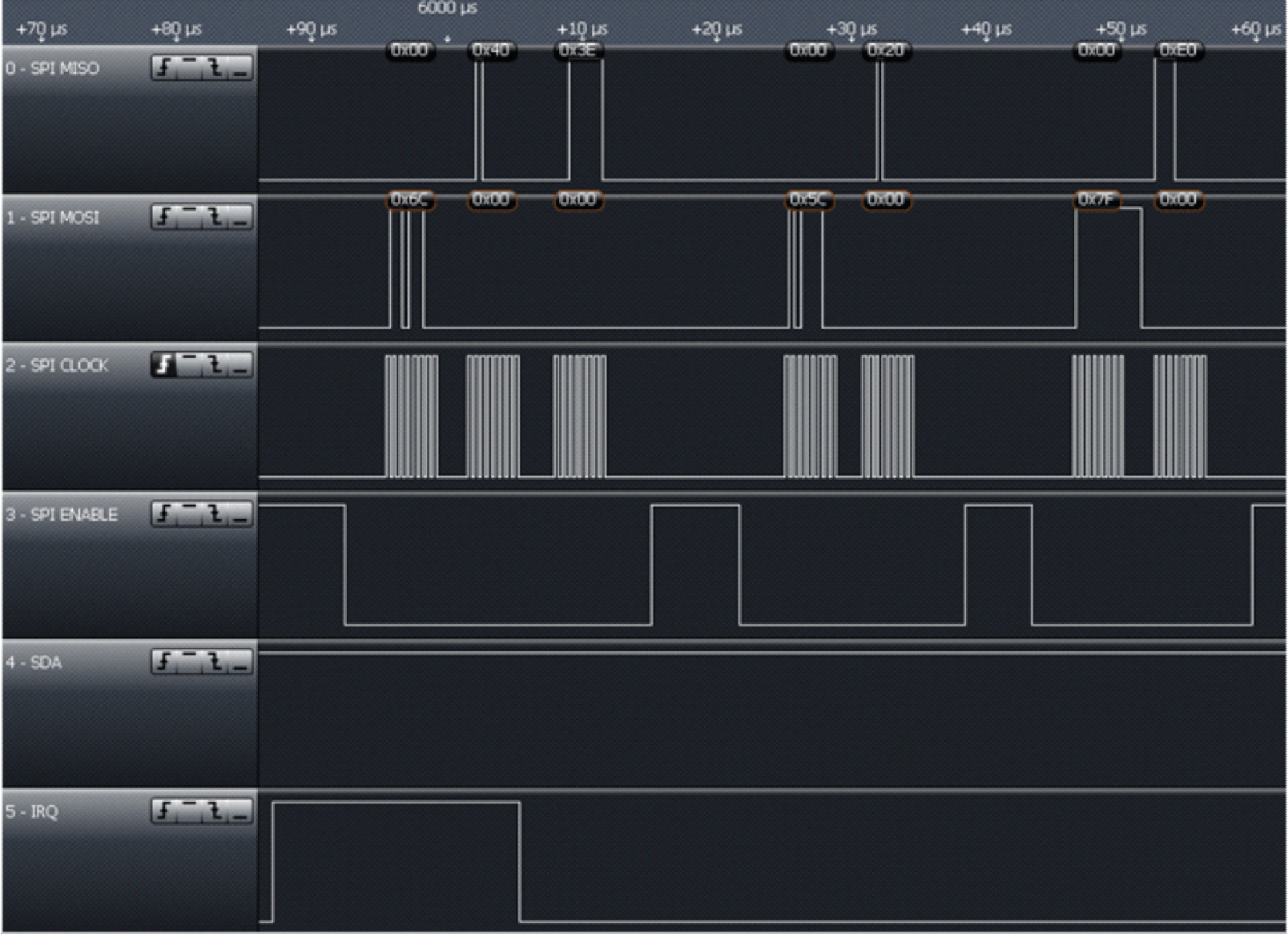 Figure 6-24 IRQ With One Byte in FIFO
TI recommends resetting the FIFO after receiving data. Additionally, the RSSI value of the tag can be read out at this time. In the example in Figure 6-25, the transponder is very close to the antenna, so a value of 0x7E is recovered.
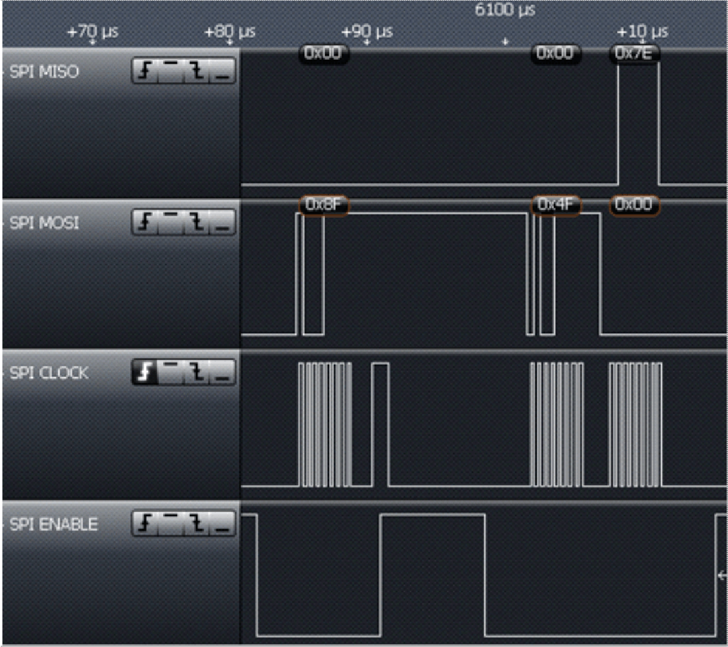 Figure 6-25 Reset FIFO and Read RSSI