ZHCS761F December 2011 – May 2017 TRF7962A
PRODUCTION DATA.
- 1器件概述
- 2修订历史记录
- 3Device Characteristics
- 4Terminal Configuration and Functions
- 5Specifications
-
6Detailed Description
- 6.1 Functional Block Diagram
- 6.2 Power Supplies
- 6.3 Supply Arrangements
- 6.4 Supply Regulator Settings
- 6.5 Power Modes
- 6.6 Receiver – Analog Section
- 6.7 Receiver – Digital Section
- 6.8 Oscillator Section
- 6.9 Transmitter - Analog Section
- 6.10 Transmitter - Digital Section
- 6.11 Transmitter – External Power Amplifier or Subcarrier Detector
- 6.12 Communication Interface
- 6.13
Direct Commands from MCU to Reader
- 6.13.1 Command Codes
- 6.13.2 Reset FIFO (0x0F)
- 6.13.3 Transmission With CRC (0x11)
- 6.13.4 Transmission Without CRC (0x10)
- 6.13.5 Transmit Next Time Slot (0x14)
- 6.13.6 Block Receiver (0x16)
- 6.13.7 Enable Receiver (0x17)
- 6.13.8 Test Internal RF (RSSI at RX Input With TX On) (0x18)
- 6.13.9 Test External RF (RSSI at RX Input With TX Off) (0x19)
- 6.13.10 Register Preset
- 6.14 Register Description
- 7Applications, Implementation, and Layout
- 8器件和文档支持
- 9机械、封装和可订购信息
6.12.7 Direct Mode
Direct mode lets the reader be configured in one of two ways:
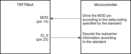
Direct mode 0 (bit 6 = 0, as defined in ISO Control register) lets the application use only the front-end functions of the reader, bypassing the protocol implementation in the reader. For transmit functions, the application has direct access to the transmit modulator through the MOD pin (pin 14). On the receive side, the application has direct access to the subcarrier signal (digitized RF envelope signal) on I/O_6 (pin 23).
Direct mode 1 (bit 6 = 1, as defined in ISO Control register) uses the subcarrier signal decoder of the selected protocol (as defined in ISO Control register). This means that the receive output is not the subcarrier signal but the decoded serial bit stream and bit clock signals. The serial data is available on I/O_6 (pin 23), and the bit clock is available on I/O_5 (pin 22). The transmit side is identical; the application has direct control over the RF modulation through the MOD input. This mode is provided so that the application can implement a protocol that has the same bit coding as one of the protocols implemented in the reader, but needs a different framing format.
To select direct mode, first choose which direct mode to enter by writing B6 in the ISO Control register. This bit determines if the receive output is the direct subcarrier signal (B6 = 0) or the serial data of the selected decoder. If B6 = 1, then the application must also define which protocol should be used for bit decoding by writing the appropriate setting in the ISO Control register.
The reader actually enters the direct mode when B6 (direct) is set to 1 in the Chip Status Control register. Direct mode starts immediately. The write command should not be terminated with a stop condition (see communication protocol), because the stop condition terminates the direct mode and clears B6. This is necessary as the direct mode uses one or two I/O pins (I/O_6 and I/O_5). Normal parallel communication is not possible in direct mode. Sending a stop condition terminates direct mode.
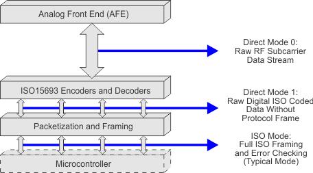
Figure 6-26 shows the different configurations available in direct mode.
- In mode 0, the reader is used as an AFE only, and protocol handling is bypassed.
- In mode 1, framing is not done, but SOF and EOF are present. This allows for a user-selectable framing level based on an existing ISO standard.
- In mode 2, data is ISO standard formatted. SOF, EOF, and error checking are removed, so the microprocessor receives only bytes of raw data through a 12-byte FIFO.
 Figure 6-26 User-Configurable Modes
The steps to enter direct mode follow, using SPI with SS communication method only as one example, as direct modes are also possible with parallel and SPI without SS. The application must enter direct mode 0 to accommodate non-ISO standard compliant card type communications. direct mode can be entered at any time, so that if a card type started with ISO standard communications, then deviated from the standard after being identified and selected, the ability to go into direct mode 0 becomes very useful.
Step 1: Configure pins I/O_0 to I/O_2 for SPI with SS
Step 2: Set pin 12 of the TRF7962A (ASK/OOK pin) to 0 for ASK or 1 for OOK
Step 3: Program the TRF7962A registers
The following registers must be explicitly set before going into direct mode.
- ISO Control register (0x01) to the appropriate standard:
- 0x02 for ISO/IEC 15693 high data rate (26.48 kbps)
- Modulator and SYS_CLK Register (0x09) to the appropriate clock speed and modulation:
- 0x21 for 6.78-MHz clock and OOK (100%) modulation
- 0x20 for 6.78-MHz clock and ASK 10% modulation
- 0x24 for 6.78-MHz clock and ASK 13% modulation
- 0x25 for 6.78-MHz clock and ASK 16% modulation
See register 0x09 definition for all other possible values.
Step 4: Enter direct mode
The following registers must be reprogrammed to enter direct mode:
- Set bit B6 of the Modulator and SYS_CLK Control register (0x09) to 1.
- Set bit B6 of the ISO Control register (0x01) to 0 for direct mode 0 (default its 0)
- Set bit B6 of the Chip Status Control register (0x00) to 1 to enter direct mode (do not send a Stop condition after this command)
- Do not terminate last write with a Stop condition. For SPI, this means that Slave Select (I/O_4) continues to stay low.
- Sending a Stop condition terminates the direct mode and clears bit B6 in the Chip Status Control register (0x00).
NOTE
NOTE
Access to registers, FIFO, and IRQ is not available during direct mode 0.
Remember that the reader enters direct mode 0 when bit 6 of the Chip Status Control register (0x00) is set to a 1, and it stays in direct mode 0 until a Stop condition is sent from the microcontroller.
NOTE
The write command should not be terminated with a Stop condition (for example, in SPI mode this is done by bringing the SS line high after the register write), because the Stop condition terminates the direct mode and clears bit 6 of the Chip Status Control register (0x00), making it a 0.
 Figure 6-27 Entering Direct Mode 0
Step 5: Transmit data using direct mode
The user now has direct control over the RF modulation through the MOD input.
 Figure 6-28 Control of RF Modulation Using MOD
The microcontroller is responsible for generating data according to the coding specified by the particular standard. The microcontroller must generate SOF, EOF, data, and CRC. In direct mode, the FIFO is not used and no IRQs are generated. See the applicable ISO standard to understand bit and frame definitions.
Step 6: Receive data using direct mode
After the TX operation is complete, the tag responds to the request and the subcarrier data is available on pin I/O_6. The microcontroller must decode the subcarrier signal according to the standard. This includes decoding the SOF, data bits, CRC, and EOF. The CRC then must be checked to verify data integrity. The receive data bytes must be buffered locally.
Step 7: Exit direct mode 0
When an EOF is received, data transmission is over, and direct mode 0 can be terminated by sending a Stop condition (the SS signal goes high). The TRF7962A returns to ISO Mode (normal mode).