ZHCS762F December 2011 – May 2017 TRF7963A
PRODUCTION DATA.
- 1器件概述
- 2修订历史记录
- 3Device Characteristics
- 4Terminal Configuration and Functions
- 5Specifications
-
6Detailed Description
- 6.1 Functional Block Diagram
- 6.2 Power Supplies
- 6.3 Supply Arrangements
- 6.4 Supply Regulator Settings
- 6.5 Power Modes
- 6.6 Receiver – Analog Section
- 6.7 Receiver – Digital Section
- 6.8 Oscillator Section
- 6.9 Transmitter - Analog Section
- 6.10 Transmitter - Digital Section
- 6.11 Transmitter – External Power Amplifier or Subcarrier Detector
- 6.12 Communication Interface
- 6.13
Direct Commands from MCU to Reader
- 6.13.1 Command Codes
- 6.13.2 Reset FIFO (0x0F)
- 6.13.3 Transmission With CRC (0x11)
- 6.13.4 Transmission Without CRC (0x10)
- 6.13.5 Block Receiver (0x16)
- 6.13.6 Enable Receiver (0x17)
- 6.13.7 Test Internal RF (RSSI at RX Input With TX On) (0x18)
- 6.13.8 Test External RF (RSSI at RX Input With TX Off) (0x19)
- 6.13.9 Register Preset
- 6.14
Register Description
- 6.14.1
Register Overview
- 6.14.1.1 Main Configuration Registers
- 6.14.1.2
Protocol Subsetting Registers
- 6.14.1.2.1 ISO14443B TX Options Register (0x02)
- 6.14.1.2.2 ISO14443A High-Bit-Rate and Parity Options Register (0x03)
- 6.14.1.2.3 TX Pulse Length Control Register (0x06)
- 6.14.1.2.4 RX No Response Wait Time Register (0x07)
- 6.14.1.2.5 RX Wait Time Register (0x08)
- 6.14.1.2.6 Modulator and SYS_CLK Control Register (0x09)
- 6.14.1.2.7 RX Special Setting Register (0x0A)
- 6.14.1.2.8 Regulator and I/O Control Register (0x0B)
- 6.14.1.3 Status Registers
- 6.14.1.4 Test Registers
- 6.14.1.5 FIFO Control Registers
- 6.14.1
Register Overview
- 7Applications, Implementation, and Layout
- 8器件和文档支持
- 9机械、封装和可订购信息
6.12.1 General Introduction
The communication interface to the reader can be configured in two ways: with a eight line parallel interface (D0:D7) plus DATA_CLK, or with a 3- or 4-wire Serial Peripheral Interface (SPI). The SPI interface uses traditional master out/slave in (MOSI), master in/slave out (MISO), IRQ, and DATA_CLK lines. The SPI can be operated with or without using the slave select line.
These communication modes are mutually exclusive, which means that only one mode can be used at a time in the application.
When the SPI interface is selected, the unused I/O_2, I/O_1, and I/O_0 pins must be hard-wired according to Table 6-6. At power up, the TRF7963A IC samples the status of these three pins and then enters one of the possible SPI modes in Table 6-6.
samples the status of these three pins. If they are not the same (all high or all low), the IC enters one of the possible SPI modes.
The TRF7963A always behaves as the slave, while the microcontroller (MCU) behaves as the master device. The MCU initiates all communications with the TRF7963A. The TRF7963A makes use of the Interrupt Request (IRQ) pin in both parallel and SPI modes to prompt the MCU for servicing attention.
Table 6-6 Pin Assignment in Parallel and Serial Interface Connection or Direct Mode
| PIN | PARALLEL | PARALLEL DIRECT | SPI WITH SS | SPI WITHOUT SS |
|---|---|---|---|---|
| DATA_CLK | DATA_CLK | DATA_CLK | DATA_CLK from master | DATA_CLK from master |
| I/O_7 | A/D[7] | MOSI(1) = data in (reader in) | MOSI(1) = data in (reader in) | |
| I/O_6 | A/D[6] | Direct mode, data out (subcarrier or bit stream) |
MISO(2) = data out (MCU out) | MISO(2) = data out (MCU out) |
| I/O_5 (3) | A/D[5] | Direct mode, strobe (bit clock out) | See (3) | See (3) |
| I/O_4 | A/D[4] | SS (slave select)(4) | – | |
| I/O_3 | A/D[3] | – | – | – |
| I/O_2 | A/D[2] | – | At VDD | At VDD |
| I/O_1 | A/D[1] | – | At VDD | At VSS |
| I/O_0 | A/D[0] | – | At VSS | At VSS |
| IRQ | IRQ interrupt | IRQ interrupt | IRQ interrupt | IRQ interrupt |
Communication is initialized by a start condition, which is expected to be followed by an Address/Command word (Adr/Cmd). The Adr/Cmd word is 8 bits long, and Table 6-7 describes its format.
Table 6-7 Address/Command Word Bit Distribution
| BIT | DESCRIPTION | BIT FUNCTION | ADDRESS | COMMAND |
|---|---|---|---|---|
| B7 | Command control bit | 0 = Address 1 = Command |
0 | 1 |
| B6 | Read/Write | 1 = Read 0 = Write |
R/W | 0 |
| B5 | Continuous address mode | 1 = Continuous mode | R/W | 0 |
| B4 | Address/command bit 4 | Adr 4 | Cmd 4 | |
| B3 | Address/command bit 3 | Adr 3 | Cmd 3 | |
| B2 | Address/command bit 2 | Adr 2 | Cmd 2 | |
| B1 | Address/command bit 1 | Adr 1 | Cmd 1 | |
| B0 | Address/command bit 0 | Adr 0 | Cmd 0 |
The MSB (bit 7) determines if the word is to be used as a command or as an address. The last two columns of Table 6-7 list the function of the separate bits if either address or command is written. Data is expected once the address word is sent. In continuous address mode (continuous mode = 1), the first data that follows the address is written (or read) to (from) the given address. For each additional data, the address is incremented by one. Continuous mode can be used to write to a block of control registers in a single stream without changing the address; for example, setup of the predefined standard control registers from the MCU nonvolatile memory to the reader. In noncontinuous address mode (simple addressed mode), only one data word is expected after the address.
Address Mode is used to write or read the configuration registers or the FIFO. When writing more than 12 bytes to the FIFO, the Continuous Address Mode should be set to 1.
The Command Mode is used to enter a command that results in reader action (for example, initialize transmission, enable reader, and turn reader on or off).
The following examples show the expected communications between an MCU and the TRF7963A.
Table 6-8 lists the format of a continuous address register read, and Figure 6-5 and Figure 6-6 show examples.
Table 6-8 Continuous Address Mode
| Start | Adr x | Data(x) | Data(x+1) | Data(x+2) | Data(x+3) | Data(x+4) | ... | Data(x+n) | StopCont |
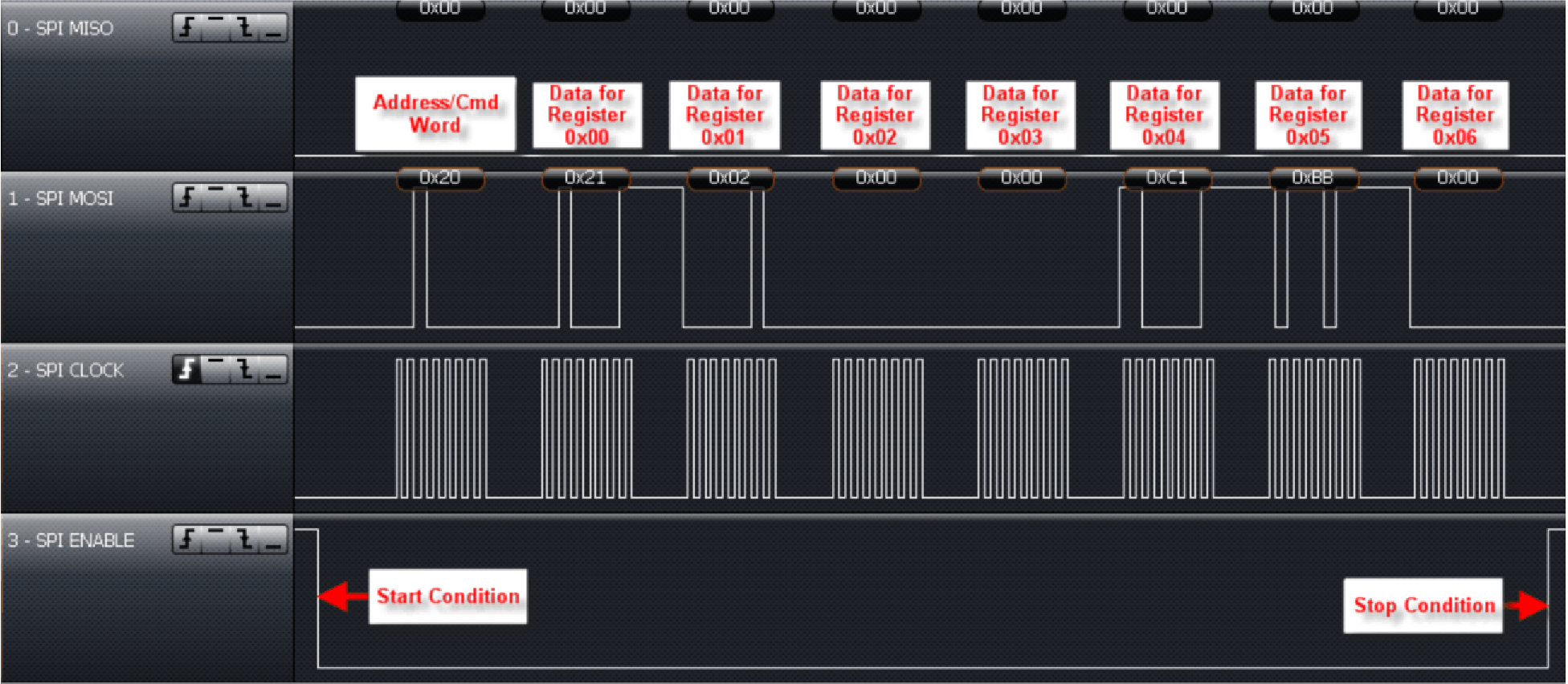 Figure 6-5 Continuous Address Register Write Example Starting With Register 0x00 (Using SPI With SS Mode)
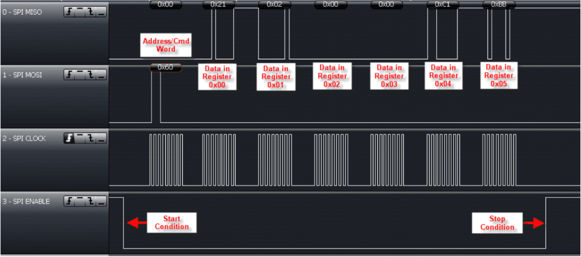 Figure 6-6 Continuous Address Register Read Example Starting With Register 0x00 (Using SPI With SS Mode)
Table 6-9 lists the format of a single address register read, and Figure 6-7 and Figure 6-8 show examples.
Table 6-9 Noncontinuous Address Mode (Single Address Mode)
| Start | Adr x | Data(x) | Adr y | Data(y) | ... | Adr z | Data(z) | StopSgl |
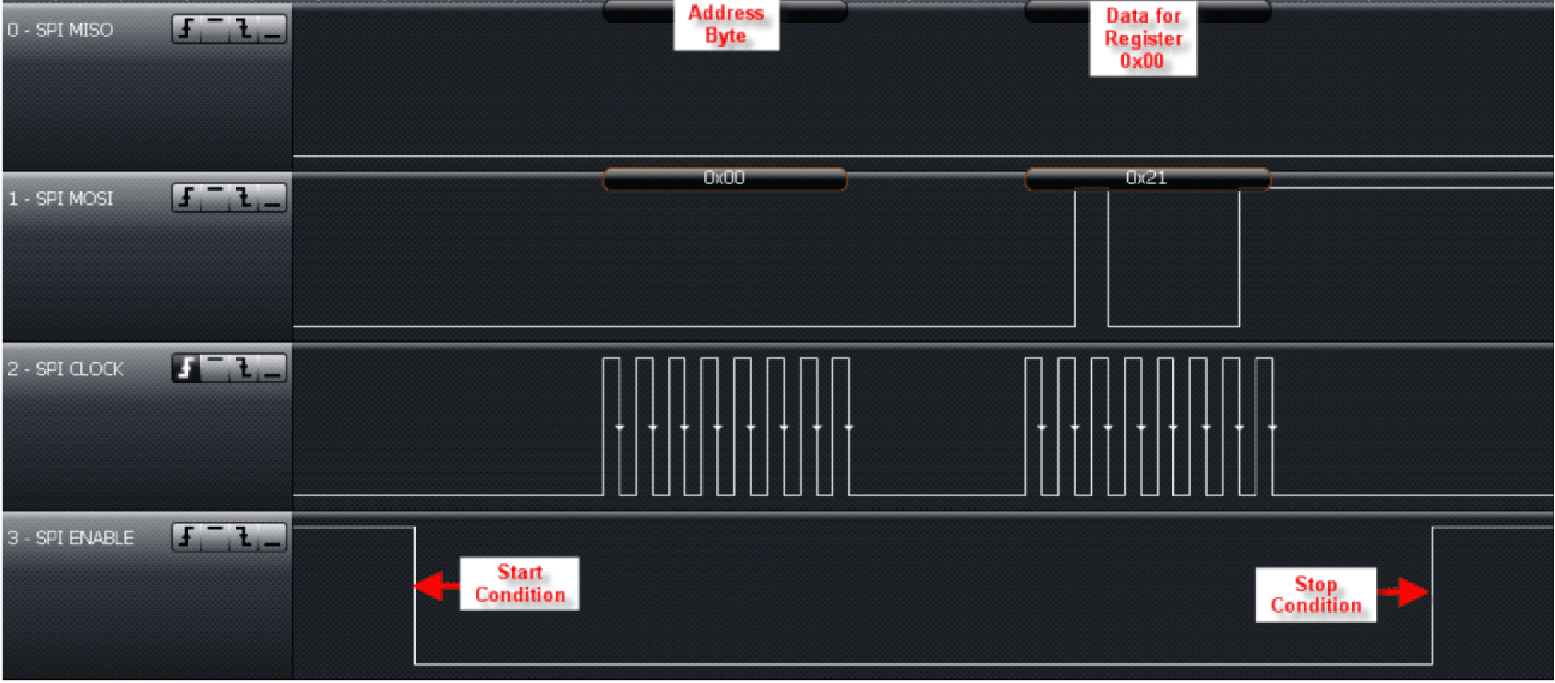 Figure 6-7 Single Address Register Write Example of Register 0x00 (Using SPI With SS Mode)
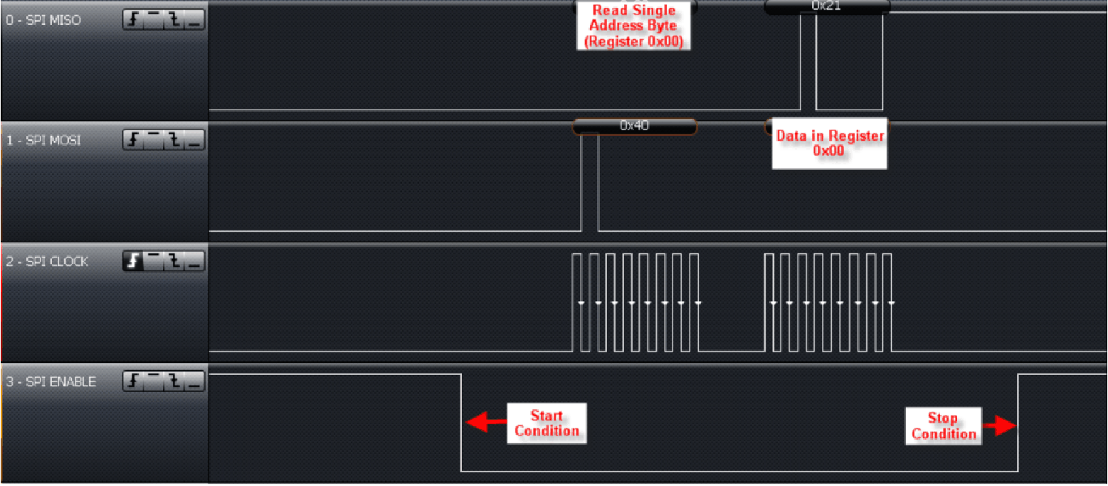 Figure 6-8 Single Address Register Read Example of Register 0x00 (Using SPI With SS Mode)
Table 6-10 lists the format of the direct command mode, and Figure 6-9 shows an example.
Table 6-10 Direct Command Mode
| Start | Cmd x | (Optional data or command) | Stop |
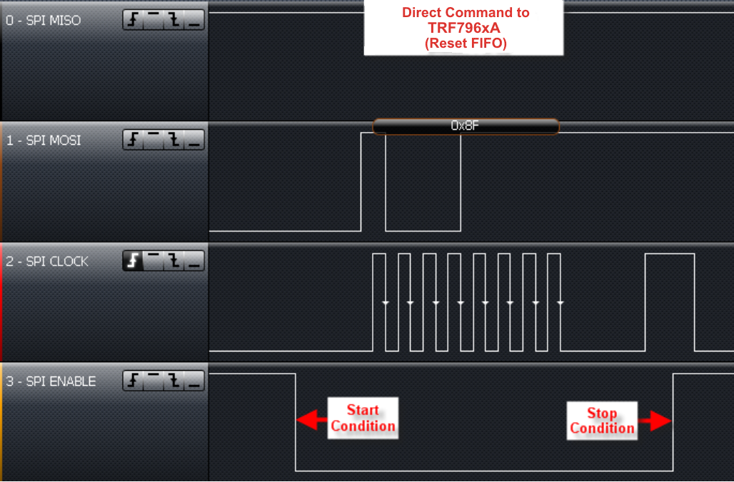 Figure 6-9 Direct Command Example of Sending 0x0F (Reset) (Using SPI With SS Mode)
The other Direct Command Codes from MCU to TRF7963A are described in Section 6.13.