ZHCS762F December 2011 – May 2017 TRF7963A
PRODUCTION DATA.
- 1器件概述
- 2修订历史记录
- 3Device Characteristics
- 4Terminal Configuration and Functions
- 5Specifications
-
6Detailed Description
- 6.1 Functional Block Diagram
- 6.2 Power Supplies
- 6.3 Supply Arrangements
- 6.4 Supply Regulator Settings
- 6.5 Power Modes
- 6.6 Receiver – Analog Section
- 6.7 Receiver – Digital Section
- 6.8 Oscillator Section
- 6.9 Transmitter - Analog Section
- 6.10 Transmitter - Digital Section
- 6.11 Transmitter – External Power Amplifier or Subcarrier Detector
- 6.12 Communication Interface
- 6.13
Direct Commands from MCU to Reader
- 6.13.1 Command Codes
- 6.13.2 Reset FIFO (0x0F)
- 6.13.3 Transmission With CRC (0x11)
- 6.13.4 Transmission Without CRC (0x10)
- 6.13.5 Block Receiver (0x16)
- 6.13.6 Enable Receiver (0x17)
- 6.13.7 Test Internal RF (RSSI at RX Input With TX On) (0x18)
- 6.13.8 Test External RF (RSSI at RX Input With TX Off) (0x19)
- 6.13.9 Register Preset
- 6.14
Register Description
- 6.14.1
Register Overview
- 6.14.1.1 Main Configuration Registers
- 6.14.1.2
Protocol Subsetting Registers
- 6.14.1.2.1 ISO14443B TX Options Register (0x02)
- 6.14.1.2.2 ISO14443A High-Bit-Rate and Parity Options Register (0x03)
- 6.14.1.2.3 TX Pulse Length Control Register (0x06)
- 6.14.1.2.4 RX No Response Wait Time Register (0x07)
- 6.14.1.2.5 RX Wait Time Register (0x08)
- 6.14.1.2.6 Modulator and SYS_CLK Control Register (0x09)
- 6.14.1.2.7 RX Special Setting Register (0x0A)
- 6.14.1.2.8 Regulator and I/O Control Register (0x0B)
- 6.14.1.3 Status Registers
- 6.14.1.4 Test Registers
- 6.14.1.5 FIFO Control Registers
- 6.14.1
Register Overview
- 7Applications, Implementation, and Layout
- 8器件和文档支持
- 9机械、封装和可订购信息
6.12.6.2 Serial Interface Mode With Slave Select (SS)
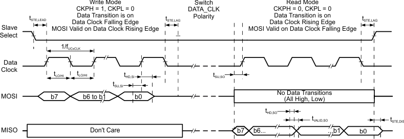
The serial interface is in reset while the Slave Select signal is high. Serial data in (MOSI) changes on the falling edge and is validated in the reader on the rising edge (see Figure 6-17). Communication is terminated when the Slave Select signal goes high.
All words must be 8 bits long with the MSB transmitted first.
 Figure 6-17 SPI With Slave Select Timing
The read command is sent out on the MOSI pin, MSB first, in the first eight clock cycles. MOSI data changes on the falling edge, and is validated in the reader on the rising edge, as shown in Figure 6-17. During the write cycle, the serial data out (MISO) is not valid. After the last read command bit (B0) is validated at the eighth rising edge of SCLK, after half a clock cycle, valid data can be read on the MISO pin at the falling edge of SCLK. It takes eight clock edges to read out the full byte (MSB first).
When using the hardware SPI (for example, an MSP430 hardware SPI) to implement this feature, care must be taken to switch the SCLK polarity after write phase for proper read operation. The example clock polarity for the Figure 6-17 shows the MSP430-specific environment in the write-mode and read-mode boxes. See the USART-SPI chapter for any specific microcontroller family for further information on the setting the appropriate clock polarity. This clock polarity switch must be done for all read (single or continuous) operations. The MOSI (serial data out) should not have any transitions (all high or all low) during the read cycle. The Slave Select should be low during the whole write and read operation.
See Section 5.6, Switching Characteristics, for the timing values shown in Figure 6-17.
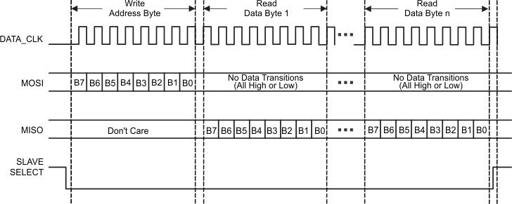
Figure 6-18 shows the continuous read operation.
 Figure 6-18 Continuous Read Operation Using SPI With Slave Select
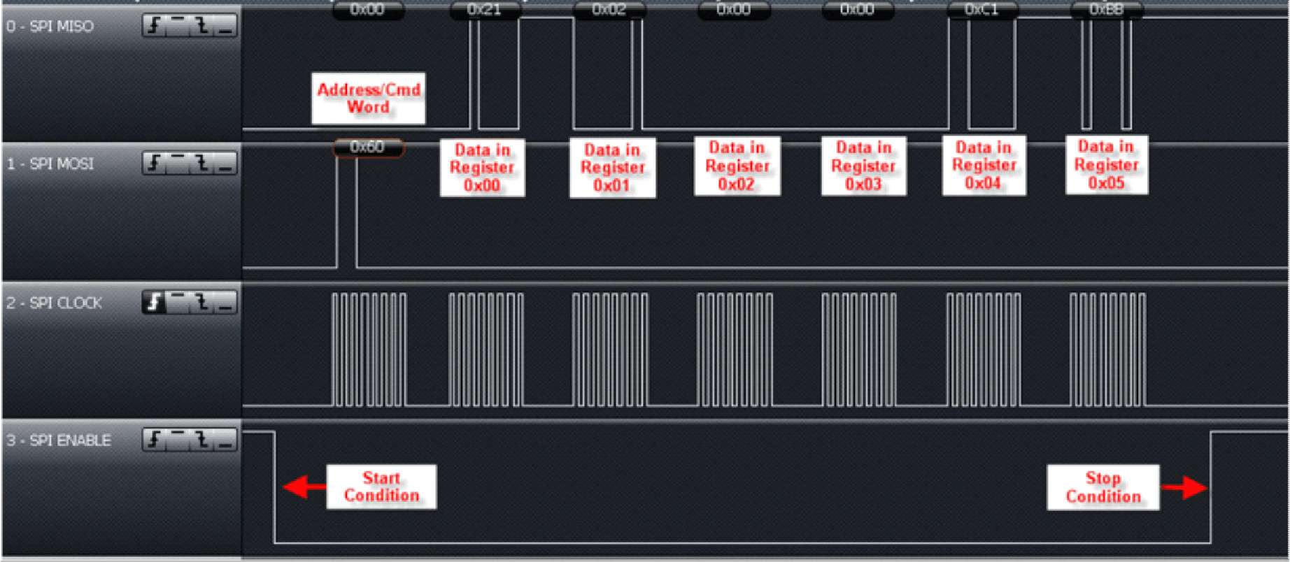
 Figure 6-19 Continuous Read of Registers 0x00 to 0x05 Using SPI With SS