ZHCSJI3H March 2007 – August 2022 TS3A24159
PRODUCTION DATA
- 1 特性
- 2 应用
- 3 说明
- 4 Revision History
- 5 Pin Configuration and Functions
-
6 Specifications
- 6.1 Absolute Maximum Ratings
- 6.2 ESD Ratings
- 6.3 Recommended Operating Conditions
- 6.4 Thermal Information
- 6.5 Electrical Characteristics for 3-V Supply
- 6.6 Electrical Characteristics for 2.5-V Supply
- 6.7 Electrical Characteristics for 1.8-V Supply
- 6.8 Switching Characteristics for a 3-V Supply
- 6.9 Switching Characteristics for a 2.5-V Supply
- 6.10 Switching Characteristics for a 1.8-V Supply
- 6.11 Typical Characteristics
- 7 Parameter Measurement Information
- 8 Detailed Description
- 9 Application and Implementation
- 10Power Supply Recommendations
- 11Layout
- 12Device and Documentation Support
- 13Mechanical, Packaging, and Orderable Information
封装选项
机械数据 (封装 | 引脚)
散热焊盘机械数据 (封装 | 引脚)
- DRC|10
订购信息
5 Pin Configuration and Functions
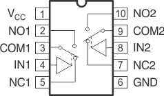
 Figure 5-1 DGS Package,10-Pin VSSOP(Top View)
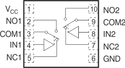
 Figure 5-2 DRC Package,10-Pin VSON(Top View)
Table 5-1 Pin Functions – VSSOP and
VSON
| PIN | TYPE(1) | DESCRIPTION | |
|---|---|---|---|
| NO. | NAME | ||
| 1 | VCC | — | Power supply |
| 2 | NO1 | I/O | Normally open signal path |
| 3 | COM1 | I/O | Common signal path |
| 4 | IN1 | I | Digital control to connect COM to NO or NC |
| 5 | NC1 | I/O | Normally closed signal path |
| 6 | GND | — | Ground |
| 7 | NC2 | I/O | Normally closed signal path |
| 8 | IN2 | I | Digital control to connect COM to NO or NC |
| 9 | COM2 | I/O | Common signal path |
| 10 | NO2 | I/O | Normally open signal path |
(1) I = input, O = output
Figure 5-3 YZP Package,10-Pin DSBGA(Bottom View)
| Legend | |
|---|---|
| Input or Output | Input |
| Ground | Power |
Table 5-2 Pin Functions – DSBGA
| PIN | TYPE(1) | DESCRIPTION | |
|---|---|---|---|
| NO. | NAME | ||
| A1 | NC1 | I/O | Normally closed signal path |
| A2 | GND | — | Ground |
| A3 | NC2 | I/O | Normally closed signal path |
| B1 | IN1 | I | Digital control to connect COM to NO or NC |
| B3 | IN2 | I | Digital control to connect COM to NO or NC |
| C1 | COM1 | I/O | Common signal path |
| C3 | COM2 | I/O | Common signal path |
| D1 | NO1 | I/O | Normally open signal path |
| D2 | VCC | — | Power supply |
| D3 | NO2 | I/O | Normally open signal path |
(1) I = input, O = output