ZHCSJI4F July 2006 – March 2015 TS3A4751
PRODUCTION DATA.
- 1 特性
- 2 应用
- 3 说明
- 4 修订历史记录
- 5 Pin Configuration and Functions
- 6 Specifications
- 7 Detailed Description
- 8 Application and Implementation
- 9 Power Supply Recommendations
- 10Layout
- 11器件和文档支持
- 12机械、封装和可订购信息
封装选项
机械数据 (封装 | 引脚)
散热焊盘机械数据 (封装 | 引脚)
订购信息
6.6 Electrical Characteristics for 3-V Supply
VCC = 2.7 V to 3.6 V, TA = –40°C to 85°C, VIH = 1.4 V, VIL = 0.5 V (unless otherwise noted).(2)(1)| PARAMETER | TEST CONDITIONS | TA | MIN | TYP(3) | MAX | UNIT | ||
|---|---|---|---|---|---|---|---|---|
| ANALOG SWITCH | ||||||||
| VCOM, VNO | Analog signal range | 0 | VCC | V | ||||
| Ron | ON-state resistance | VCC = 2.7 V, ICOM = –100 mA,
VNO = 1.5 V |
25°C | 0.7 | 0.9 | Ω | ||
| Full | 1.1 | |||||||
| ΔRon | ON-state resistance match between channels(4) | VCC = 2.7 V, ICOM = –100 mA,
VNO = 1.5 V |
25°C | 0.03 | 0.05 | Ω | ||
| Full | 0.15 | |||||||
| Ron(flat) | ON-state resistance flatness(5) | VCC = 2.7 V, ICOM = –100 mA,
VNO = 1 V, 1.5 V, 2 V |
25°C | 0.23 | 0.4 | Ω | ||
| Full | 0.5 | |||||||
| INO(OFF) | NO
OFF leakage current(6) |
VCC = 3.6 V, VCOM = 0.3 V, 3 V,
VNO = 3 V, 0.3 V |
25°C | –2 | 1 | 2 | nA | |
| Full | –18 | 18 | ||||||
| ICOM(OFF) | COM
OFF leakage current(6) |
VCC = 3.6 V, VCOM = 0.3 V, 3 V,
VNO = 3 V, 0.3 V |
25°C | –2 | 1 | 2 | nA | |
| Full | –18 | 18 | ||||||
| ICOM(ON) | COM
ON leakage current(6) |
VCC = 3.6 V, VCOM = 0.3 V, 3 V,
VNO = 0.3 V, 3 V, or floating |
25°C | –2.5 | 0.01 | 2.5 | nA | |
| Full | –5 | 5 | ||||||
| DYNAMIC | ||||||||
| tON | Turn-on time | VNO = 1.5 V, RL = 50 Ω,
CL = 35 pF, See Figure 1 |
25°C | 5 | 14 | ns | ||
| Full | 15 | |||||||
| tOFF | Turn-off time | VNO = 1.5 V, RL = 50 Ω,
CL = 35 pF, See Figure 1 |
25°C | 4 | 9 | ns | ||
| Full | 10 | |||||||
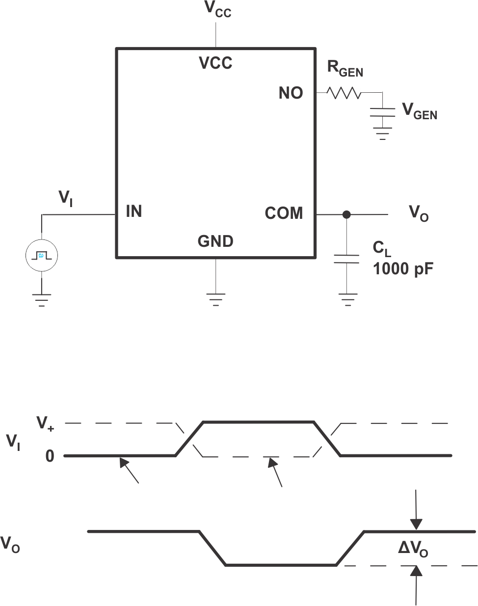
| QC | Charge injection | VGEN = 0, RGEN = 0, CL = 1 nF,
See Figure 5 |
25°C | 3 | pC | |||
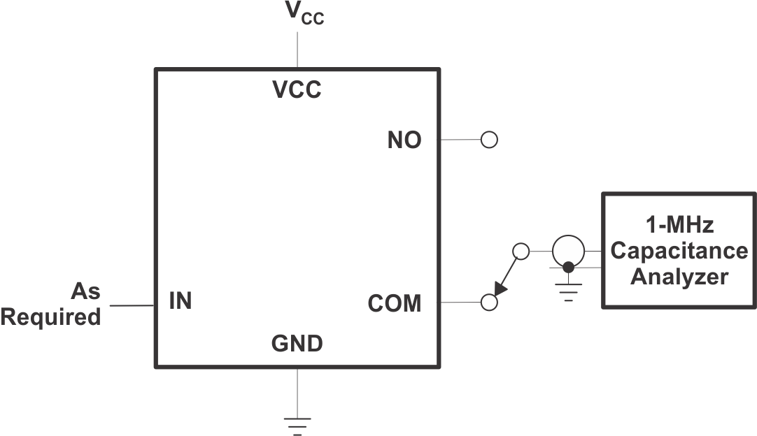
| CNO(OFF) | NO OFF capacitance | f = 1 MHz, See Figure 2 | 25°C | 23 | pF | |||
| CCOM(OFF) | COM OFF capacitance | f = 1 MHz, See Figure 2 | 25°C | 20 | pF | |||
| CCOM(ON) | COM ON capacitance | f = 1 MHz, See Figure 2 | 25°C | 43 | pF | |||
| BW | Bandwidth | RL = 50 Ω, Switch ON | 25°C | 125 | MHz | |||
| OISO | OFF isolation(7) | RL = 50 Ω, CL = 5 pF,
See Figure 3 |
f = 10 MHz | 25°C | –40 | dB | ||
| f = 1 MHz | –62 | |||||||
| XTALK | Crosstalk | RL = 50 Ω, CL = 5 pF,
See Figure 3 |
f = 10 MHz | 25°C | –73 | dB | ||
| f = 1 MHz | –95 | |||||||
| THD | Total harmonic distortion | f = 20 Hz to 20 kHz, VCOM = 2 VP-P | RL = 32 Ω | 25°C | 0.04% | |||
| RL = 600 Ω | 0.003% | |||||||
| DIGITAL CONTROL INPUTS (IN1–IN4) | ||||||||
| VIH | Input logic high | Full | 1.4 | V | ||||
| VIL | Input logic low | Full | 0.5 | V | ||||
| IIN | Input leakage current | VI = 0 or VCC | 25°C | 0.5 | 1 | nA | ||
| Full | –20 | 20 | ||||||
| SUPPLY | ||||||||
| VCC | Power-supply range | 1.6 | 3.6 | V | ||||
| ICC | Positive-supply current | VCC = 3.6 V, VIN = 0 or VCC | 25°C | 0.075 | μA | |||
| Full | 0.75 | |||||||
(1) Parts are tested at 85°C and specified by design and correlation over the full temperature range.
(2) The algebraic convention, whereby the most negative value is a minimum and the most positive value is a maximum.
(3) Typical values are at VCC = 3 V, TA = 25°C.
(4) Δron = ron(max) – ron(min)
(5) Flatness is defined as the difference between the maximum and minimum value of ron as measured over the specified analog signal ranges.
(6) Leakage parameters are 100% tested at the maximum-rated hot operating temperature and specified by correlation at TA = 25°C.
(7) OFF isolation = 20log10 (VCOM/VNO), VCOM = output, VNO = input to OFF switch
 Figure 1. Switching Times
  Figure 2. NO and COM Capacitance
  Figure 3. OFF Isolation, Bandwidth, and Crosstalk
A. CL includes probe and jig capacitance.
Figure 4. Total Harmonic Distortion (THD)  Figure 5. Charge Injection (QC)