ZHCSIB0H January 2005 – May 2018 TS3A5018
PRODUCTION DATA.
- 1 特性
- 2 应用
- 3 说明
- 4 修订历史记录
- 5 Pin Configuration and Functions
-
6 Specifications
- 6.1 Absolute Maximum Ratings
- 6.2 ESD Ratings
- 6.3 Recommended Operating Conditions
- 6.4 Thermal Information
- 6.5 Electrical Characteristics for 3.3-V Supply
- 6.6 Electrical Characteristics for 2.5-V Supply
- 6.7 Electrical Characteristics for 2.1-V Supply
- 6.8 Electrical Characteristics for 1.8-V Supply
- 6.9 Switching Characteristics for 3.3-V Supply
- 6.10 Switching Characteristics for 2.5-V Supply
- 6.11 Switching Characteristics for 1.8-V Supply
- 6.12 Typical Characteristics
- 7 Parameter Measurement Information
- 8 Detailed Description
- 9 Application and Implementation
- 10Power Supply Recommendations
- 11Layout
- 12器件和文档支持
- 13机械、封装和可订购信息
封装选项
请参考 PDF 数据表获取器件具体的封装图。
机械数据 (封装 | 引脚)
- PW|16
- DBQ|16
- RGY|16
- D|16
- DGV|16
- RSV|16
散热焊盘机械数据 (封装 | 引脚)
- RGY|16
订购信息
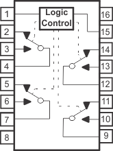
5 Pin Configuration and Functions
D, DBQ, DGV and PW Package
16-Pin SOIC, SSOP, TVSOP and TSSOP
(Top View)
Logic Circuit

RGY Package
16-Pin VQFN
(Top View)
RSV Package
16-Pin UQFN
(Top View)
Pin Functions
| PIN | TYPE | DESCRIPTION | ||
|---|---|---|---|---|
| NAME | SOIC, SSOP, TVSOP, VQFN NO. | UQFN NO. | ||
| COM1 | 4 | 2 | I/O | Common path for switch |
| COM2 | 7 | 5 | I/O | Common path for switch |
| COM3 | 9 | 7 | I/O | Common path for switch |
| COM4 | 12 | 10 | I/O | Common path for switch |
| EN | 15 | 13 | I | Active-low switch enable input |
| GND | 8 | 6 | — | Ground |
| IN | 1 | 15 | I | Switch path selector input |
| NC1 | 2 | 16 | I/O | Normally closed path for switch |
| NC2 | 5 | 3 | I/O | Normally closed path for switch |
| NC3 | 11 | 9 | I/O | Normally closed path for switch |
| NC4 | 14 | 12 | I/O | Normally closed path for switch |
| NO1 | 3 | 1 | I/O | Normally open path for switch |
| NO2 | 6 | 4 | I/O | Normally open path for switch |
| NO3 | 10 | 8 | I/O | Normally open path for switch |
| NO4 | 13 | 11 | I/O | Normally open path for switch |
| V+ | 16 | 14 | — | Supply voltage |