ZHCSAQ2B January 2013 – April 2017 TS3A5223
PRODUCTION DATA.
9 Application and Implementation
NOTE
Information in the following applications sections is not part of the TI component specification, and TI does not warrant its accuracy or completeness. TI’s customers are responsible for determining suitability of components for their purposes. Customers should validate and test their design implementation to confirm system functionality.
9.1 Application Information
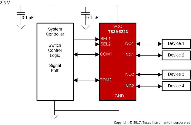
The TS3A5223 switch is bidirectional, so the NO, NC and COM pins can be used as either inputs or outputs. This switch is typically used when there is only one signal path that needs to be able to communicate to 2 different signal paths.
9.2 Typical Application
 Figure 13. Typical Application
9.2.1 Design Requirements
The TS3A5223 can be properly operated without any external components.
Unused, pins COM, NC, and NO may be left floating or grounded.
Digital control pins IN must be pulled up to VCC or down to GND to avoid undesired switch positions that could result from the floating pin and cause excess current consumption. For more information, refer to the application note Implications of Slow or Floating CMOS Inputs (SCBA002).
9.2.2 Detailed Design Procedure
Ensure that all of the signals passing through the switch are within the ranges specified in Recommended Operating Conditions to ensure proper performance.
9.2.3 Application Curves

| VCC = 3.6 V |