ZHCSJR6B SEPTEMBER   2004  – October 2019 TS3L110

PRODUCTION DATA.  

  1. 特性
  2. 应用
  3. 说明
    1.     逻辑图(正逻辑)
  4. 修订历史记录
  5. Pin Configuration and Functions
    1.     Pin Functions
  6. Specifications
    1. 6.1 Absolute Maximum Ratings
    2. 6.2 ESD Ratings
    3. 6.3 Recommended Operating Conditions
    4. 6.4 Thermal Information
    5. 6.5 Electrical Characteristics
    6. 6.6 Switching Characteristics
    7. 6.7 Dynamic Characteristics
    8. 6.8 Typical Characteristics
  7. Parameter Measurement Information
  8. Detailed Description
    1. 8.1 Overview
    2. 8.2 Functional Block Diagram
    3. 8.3 Feature Description
    4. 8.4 Device Functional Modes
  9. Application and Implementation
    1. 9.1 Application Information
    2. 9.2 Typical Application
      1. 9.2.1 Design Requirements
      2. 9.2.2 Detailed Design Procedure
      3. 9.2.3 Application Curves
  10. 10Power Supply Recommendations
  11. 11Layout
    1. 11.1 Layout Guidelines
    2. 11.2 Layout Example
  12. 12器件和文档支持
    1. 12.1 接收文档更新通知
    2. 12.2 社区资源
    3. 12.3 商标
    4. 12.4 静电放电警告
    5. 12.5 Glossary
  13. 13机械、封装和可订购信息

封装选项

请参考 PDF 数据表获取器件具体的封装图。

机械数据 (封装 | 引脚)
  • PW|16
  • DBQ|16
  • RGY|16
  • D|16
  • DGV|16
散热焊盘机械数据 (封装 | 引脚)
订购信息

Parameter Measurement Information

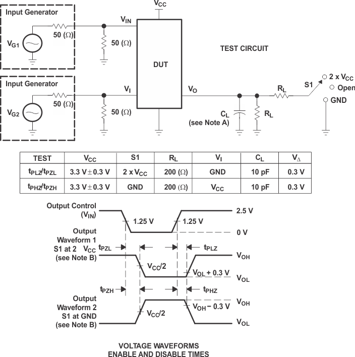
TS3L110 tstcnd1_cds176.gif
CL includes probe and jig capacitance.
Waveform 1 is for an output with internal conditions such that the output is low. Waveform 2 is for an output with internal conditions such that the output is high, except when disabled by the output control.
All input pulses are supplied by generators having the following characteristics: PRR ≤ 10 MHz, ZO = 50 Ω, tr ≤ 2.5 ns, tf ≤ 2.5 ns.
The outputs are measured one at a time, with one transition per measurement.
tPLZ and tPHZ are the same as tdis.
tPLZ and tPHH are the same as ten.
Figure 5. Test Circuit and Voltage Waveforms
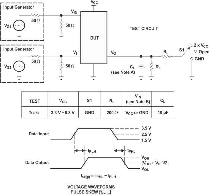
TS3L110 tstcnd2_cds176.gif
CL includes probe and jig capacitance.
Switch is ON during the measurement of tsk(p), that is, voltage at E = 0 and S = VCC or GND.
Figure 6. Test Circuit and Voltage Waveforms
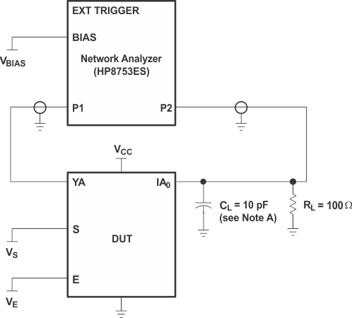
TS3L110 tstcir1_cds176.gif
CL includes probe and jig capacitance.
Figure 7. Test Circuit for Frequency Response (BW)

Frequency response is measured at the output of the ON channel. For example, when VS = 0, VE = 0, and YA is the input, the output is measured at IA0. All unused analog I/O ports are left open.

HP8753ES Setup

  • Average = 4
  • RBW = 3 kHz
  • VBIAS = 0.35 V
  • ST = 2 s
  • P1 = 0 dBM

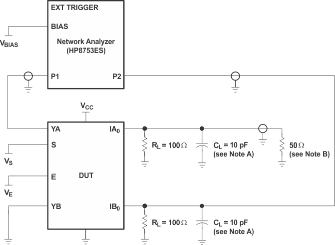
TS3L110 tstcir2_cds176.gif
CL includes probe and jig capacitance.
A 50-Ω termination resistor is needed to match the loading of the network analyzer
Figure 8. Test Circuit for Crosstalk (XTALK)

Crosstalk is measured at the output of the nonadjacent ON channel. For example, when VS = 0, VE = 0, and YA is the input, the output is measured at IB0. All unused analog input (Y) ports are connected to GND, and output (I) ports are connected to GND through 50-Ω pulldown resistors.

HP8753ES Setup

  • Average = 4
  • RBW = 3 kHz
  • VBIAS = 0.35 V
  • ST = 2 s
  • P1 = 0 dBM

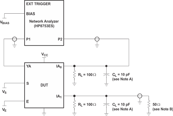
TS3L110 tstcir3_cds176.gif
CL includes probe and jig capacitance.
A 50-Ω termination resistor is needed to match the loading of the network analyzer
Figure 9. Test Circuit for OFF Isolation (OIRR)

OFF isolation is measured at the output of the OFF channel. For example, when VS = VCC, VE = 0, and YA is the input, the output is measured at IA0. All unused analog input (Y) ports are left open, and output (I) ports are connected to GND through 50-Ω pulldown resistors.

HP8753FS Setup

  • Average = 4
  • RBW = 3 kHz
  • VBIAS = 0.35 V
  • ST = 2 s
  • P1 = 0 dBM