ZHCSJR6B SEPTEMBER 2004 – October 2019 TS3L110
PRODUCTION DATA.
- 1 特性
- 2 应用
- 3 说明
- 4 修订历史记录
- 5 Pin Configuration and Functions
- 6 Specifications
- 7 Parameter Measurement Information
- 8 Detailed Description
- 9 Application and Implementation
- 10Power Supply Recommendations
- 11Layout
- 12器件和文档支持
- 13机械、封装和可订购信息
封装选项
请参考 PDF 数据表获取器件具体的封装图。
机械数据 (封装 | 引脚)
- PW|16
- DBQ|16
- RGY|16
- D|16
- DGV|16
散热焊盘机械数据 (封装 | 引脚)
- RGY|16
订购信息
11.1 Layout Guidelines
- TI recommends keeping the high-speed signals as short as possible.
- Each via introduces discontinuities in the transmission line of the signal and increases the chance of picking up interference from the other layers of the board. Be careful when designing test points on twisted pair lines; through-hole pins are not recommended.
- When it becomes necessary to turn 90°, use two 45° turns or an arc instead of making a single 90° turn. This reduces reflections on the signal traces by minimizing impedance discontinuities.
- Do not route traces under or near crystals, oscillators, clock signal generators, switching regulators, mounting holes, magnetic devices or ICs that use or duplicate clock signals.
- Avoid stubs on the high-speed signals because they cause signal reflections. If a stub is unavoidable, then the stub must be less than 200 mm.
- Route all high-speed signal traces over continuous GND planes, with no interruptions. Avoid crossing over anti-etch, commonly found with plane splits.
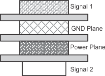
- Due to high-frequency signals, a printed-circuit board with at least four layers is recommended; two signal layers separated by a ground and power layer as shown in Figure 12.
- The majority of signal traces must run on a single layer, preferably Signal 1. Immediately next to this layer should be the GND plane, which is solid with no cuts. Avoid running signal traces across a split in the ground or power plane. When running across split planes is unavoidable, sufficient decoupling must be used. Minimizing the number of signal vias reduces EMI by reducing inductance at high frequencies.
 Figure 12. Four-Layer Board Stackup