ZHCSAJ9F December 2012 – June 2019 TS3USB3000
PRODUCTION DATA.
8.3.2 Overvoltage Protection When 9-V Short to D+/– Pin
This section describes how to protect the TS3USB3000 and the surrounding system when the D+/– pin is exposed to voltages greater than 5 V and less than 9 V. Voltages higher than 9 V damages the device.
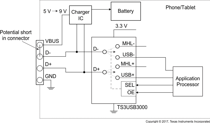
In charging applications it is possible for the USB plug to be inserted in such a way that the VBUS pin shorts to the D+/– pin of the connector. If there are peripherals on the D+/– pin that cannot tolerate conditions up to 9 V they can be damaged or destroyed. The TS3USB3000 can be used to protect the system from excess voltage if the correct precautions are taken.
In Figure 13, the system has an application processor (AP) that cannot survive 9 V on the USB data lines. The following procedure protects the system and the TS3USB3000. As stated in the Absolute Maximum Ratings table footnotes, the 9 V rating is only applicable while the VCC is powered within the voltage range of the recommended operating conditions and the OE pin is high.
- After a charger is connected to the USB port, the AP detects that a DCP is attached.
- The AP pulls the OE pin high to disable the switches.
- The AP communicates to the Charger that it can negotiate for a faster charging mode with VBUS at 9 V.
- The TS3USB3000 is now in a low-power state with the switches disabled and can protect the AP.
 Figure 13. Potential VBUS to D+/– Short Example