ZHCSBM1D September   2013  – August 2024 TS3USB3031

PRODUCTION DATA  

  1.   1
  2. 特性
  3. 应用
  4. 说明
  5. Pin Configuration and Functions
  6. Specifications
    1. 5.1 Absolute Maximum Ratings
    2. 5.2 ESD Ratings
    3. 5.3 Recommended Operating Conditions
    4. 5.4 Thermal Information
    5. 5.5 Electrical Characteristics
    6. 5.6 Dynamic Characteristics
    7. 5.7 Typical Characteristics
  7.   Parameter Measurement Information
  8. Detailed Description
    1. 6.1 Overview
    2. 6.2 Functional Block Diagram
    3. 6.3 Feature Description
      1. 6.3.1 IOFF Protection
      2. 6.3.2 1.8-V Compatible Logic
      3. 6.3.3 Overvoltage Tolerant (OVT)
    4. 6.4 Device Functional Modes
  9. Application and Implementation
    1. 7.1 Application Information
    2. 7.2 Typical Application
      1. 7.2.1 Design Requirements
      2. 7.2.2 Detailed Design Procedure
      3. 7.2.3 Application Curves
        1. 7.2.3.1 MHL Eye Pattern
        2. 7.2.3.2 USB EYE Pattern
    3. 7.3 Power Supply Recommendations
    4. 7.4 Layout
      1. 7.4.1 Layout Guidelines
      2. 7.4.2 Layout Example
  10. Device and Documentation Support
    1. 8.1 Documentation Support
      1. 8.1.1 Related Documentation
    2. 8.2 接收文档更新通知
    3. 8.3 支持资源
    4. 8.4 Trademarks
    5. 8.5 静电放电警告
    6. 8.6 术语表
  11. Revision History
  12. 10Mechanical, Packaging, and Orderable Information

封装选项

机械数据 (封装 | 引脚)
散热焊盘机械数据 (封装 | 引脚)
订购信息

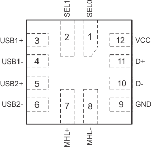
Pin Configuration and Functions

TS3USB3031 RMG Package, 12-Pin VQFN
                        (Top View)Figure 4-1 RMG Package, 12-Pin VQFN (Top View)
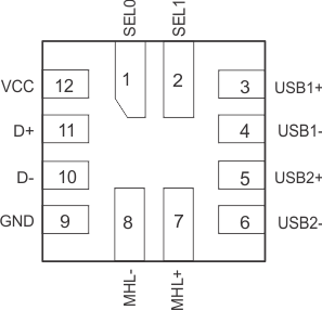
TS3USB3031 RMG Package, 12-Pin VQFN
                        (Bottom View)Figure 4-2 RMG Package, 12-Pin VQFN (Bottom View)
Table 4-1 Pin Functions
PIN TYPE(1) DESCRIPTION
NAME NO.
SEL0 1 I Digital control Input
SEL1 2 I Digital control Input
USB1+ 3 I/O Differential signal path 1
USB1– 4 I/O Differential signal path 1
USB2+ 5 I/O Differential signal path 2
USB2– 6 I/O Differential signal path 2
MHL+ 7 I/O Differential signal path 3
MHL– 8 I/O Differential signal path 3
GND 9 G Ground
D– 10 I/O Common Differential signal path
D+ 11 I/O Common Differential signal path
VCC 12 P Power Supply
G = Ground, I = Input, O = Output, P = Power