SCDS256A October 2009 – September 2016 TS3USB31E
PRODUCTION DATA.
- 1 Features
- 2 Applications
- 3 Description
- 4 Revision History
- 5 Pin Configuration and Functions
- 6 Specifications
- 7 Application Information
- 8 Parameter Measurement Information
- 9 Detailed Description
- 10Application and Implementation
- 11Power Supply Recommendations
- 12Layout
- 13Device and Documentation Support
- 14Mechanical, Packaging, and Orderable Information
9 Detailed Description
9.1 Overview
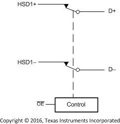
The TS3USB31E is a 1:1 SPST high-bandwidth switch specially designed for the switching of high-speed USB 2.0 signals. The switch is bidirectional and offers little or no attenuation of the high-speed signals. It is designed for low bit-to-bit skew and high channel-to-channel noise isolation, and is compatible with various standards, such as high-speed USB 2.0 (480 Mbps).
9.2 Functional Block Diagram

9.3 Feature Description
9.3.1 IOFF Supports Partial Power-Down Mode Operation
When VCC = 0 V, the signal path is placed in a high impedance state which isolates the bus. This allows signals to be present on the D± and HSD± pins before the device is powered up without damaging the device.
9.4 Device Functional Modes
The TS3USB31E device has two modes that are digitally controlled by the OE pin. Setting the OE pin High isolates the signal path by a high impedance state. See Table 1.
Table 1. Truth Table
| OE | FUNCTION |
|---|---|
| H | Disconnect |
| L | D+, D– = HSD+, HSD– |