ZHCSIM3F January 2005 – August 2018 TS5A2066
PRODUCTION DATA.
- 1 特性
- 2 应用
- 3 说明
- 4 修订历史记录
- 5 Pin Configuration and Functions
-
6 Specifications
- 6.1 Absolute Maximum Ratings
- 6.2 ESD Ratings
- 6.3 Recommended Operating Conditions
- 6.4 Thermal Information
- 6.5 Electrical Characteristics For 5-V Supply
- 6.6 Electrical Characteristics For 3.3-V Supply
- 6.7 Electrical Characteristics For 2.5-V Supply
- 6.8 Electrical Characteristics For 1.8-V Supply
- 6.9 Typical Performance
- 7 Parameter Measurement Information
- 8 Detailed Description
- 9 Application and Implementation
- 10Power Supply Recommendations
- 11Layout
- 12器件和文档支持
- 13机械、封装和可订购信息
封装选项
请参考 PDF 数据表获取器件具体的封装图。
机械数据 (封装 | 引脚)
- DCU|8
- YZP|8
- DCT|8
散热焊盘机械数据 (封装 | 引脚)
订购信息
7 Parameter Measurement Information
Table 1. Parameter Description
| SYMBOL | DESCRIPTION |
|---|---|
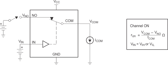
| VCOM | Voltage at COM |
| VNO | Voltage at NO |
| ron | Resistance between COM and NO ports when the channel is ON |
| Δron | Difference of ron between channels in a specific device |
| ron(flat) | Difference between the maximum and minimum value of ron in a channel over the specified range of conditions |
| INO(OFF) | Leakage current measured at the NO port, with the corresponding channel (NO to COM) in the OFF state |
| INO(ON) | Leakage current measured at the NO port, with the corresponding channel (NO to COM) in the ON state and the output (COM) open |
| ICOM(OFF) | Leakage current measured at the COM port, with the corresponding channel (COM to NO) in the OFF state |
| ICOM(ON) | Leakage current measured at the COM port, with the corresponding channel (COM to NO) in the ON state and the output (NO) open |
| VIH | Minimum input voltage for logic high for the control input (IN) |
| VIL | Maximum input voltage for logic low for the control input (IN) |
| VIN | Voltage at the control input (IN) |
| IIH, IIL | Leakage current measured at the control input (IN) |
| tON | Turn-on time for the switch. This parameter is measured under the specified range of conditions and by the propagation delay between the digital control (IN) signal and analog output (COM or NO) signal when the switch is turning ON. |
| tOFF | Turn-off time for the switch. This parameter is measured under the specified range of conditions and by the propagation delay between the digital control (IN) signal and analog output (COM or NO) signal when the switch is turning OFF. |
| QC | Charge injection is a measurement of unwanted signal coupling from the control (IN) input to the analog (NO or COM) output. This is measured in coulomb (C) and measured by the total charge induced due to switching of the control input. Charge injection, QC = CL × ΔVCOM, CL is the load capacitance and ΔVCOM is the change in analog output voltage. |
| CNO(OFF) | Capacitance at the NO port when the corresponding channel (NO to COM) is OFF |
| CNO(ON) | Capacitance at the NO port when the corresponding channel (NO to COM) is ON |
| CCOM(OFF) | Capacitance at the COM port when the corresponding channel (COM to NO) is OFF |
| CCOM(ON) | Capacitance at the COM port when the corresponding channel (COM to NO) is ON |
| CIN | Capacitance of IN |
| OISO | OFF isolation of the switch is a measurement of OFF-state switch impedance. This is measured in dB in a specific frequency, with the corresponding channel (NO to COM) in the OFF state. |
| XTALK | Crosstalk is a measurement of unwanted signal coupling from an ON channel to an adjacent ON channel (NC1 to NC2). This is measured in a specific frequency and in dB. |
| BW | Bandwidth of the switch. This is the frequency in which the gain of an ON channel is –3 dB below the DC gain. |
| THD | Total harmonic distortion is defined as the ratio of the root mean square (RMS) value of the second, third, and higher harmonics to the magnitude of fundamental harmonic. |
| ICC | Static power-supply current with the control (IN) pin at VCC or GND |
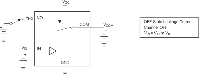 Figure 17. OFF-State Leakage Current (ICOM(OFF), INO(OFF))
 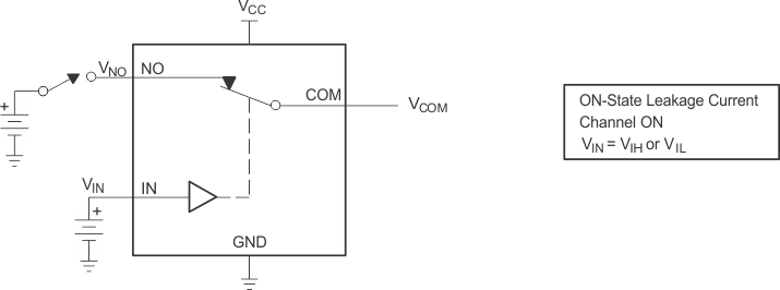 Figure 18. ON-State Leakage Current (ICOM(ON), INO(ON))
 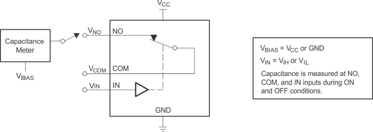 Figure 19. Capacitance (CIN, CCOM(OFF), CCOM(ON), CNO(OFF), CNO(ON))
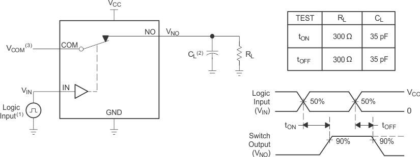
1. All input pulses are supplied by generators having the following characteristics: PRR ≤ 10 MHz, ZO = 50 Ω, tr < 5 ns,
tf < 5 ns.
tf < 5 ns.
2. CL includes probe and jig capacitance.
3. See Electrical Characteristics tables for VCOM.
Figure 20. Turn-On (tON) and Turn-Off Time (tOFF) 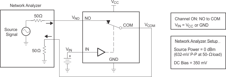 Figure 21. Bandwidth (BW)
  Figure 22. OFF Isolation (OISO)
  Figure 23. Crosstalk (XTALK)
1. All input pulses are supplied by generators having the following characteristics: PRR ≤ 10 MHz, ZO = 50 Ω, tr < 5 ns,
tf < 5 ns.
tf < 5 ns.
2. CL includes probe and jig capacitance.
Figure 24. Charge Injection (QC) 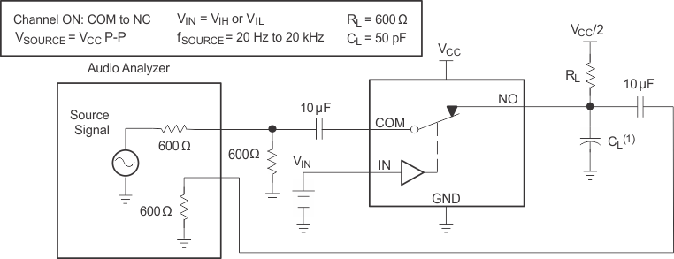
1. CL includes probe and jig capacitance.
Figure 25. Total Harmonic Distortion (THD) 