SCDS285B March 2009 – August 2016 TS5A21366
PRODUCTION DATA.
- 1 Features
- 2 Applications
- 3 Description
- 4 Revision History
- 5 Pin Configuration and Functions
-
6 Specifications
- 6.1 Absolute Maximum Ratings
- 6.2 ESD Ratings
- 6.3 Recommended Operating Conditions
- 6.4 Thermal Information
- 6.5 Electrical Characteristics for 5-V Supply
- 6.6 Electrical Characteristics for 3.3-V Supply
- 6.7 Electrical Characteristics for 2.5-V Supply
- 6.8 Electrical Characteristics for 1.8-V Supply
- 6.9 Typical Characteristics
- 7 Parameter Measurement Information
- 8 Detailed Description
- 9 Application and Implementation
- 10Power Supply Recommendations
- 11Layout
- 12Device and Documentation Support
- 13Mechanical, Packaging, and Orderable Information
9 Application and Implementation
NOTE
Information in the following applications sections is not part of the TI component specification, and TI does not warrant its accuracy or completeness. TI’s customers are responsible for determining suitability of components for their purposes. Customers should validate and test their design implementation to confirm system functionality.
9.1 Application Information
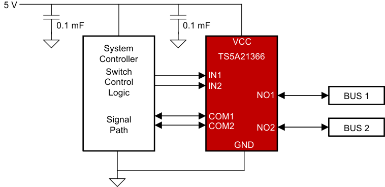
2-channel SPST analog switches are used to provide bus isolation in the system by turning on and off a signal path. The TS5A21366 is selected for applications needing to isolate analog signals where signal integrity is most important because of the switches' low on-state resistance and low on-state leakage performance. An example of this type of application is an analog signal from a sensor into an ADC.
9.2 Typical Application
 Figure 26. Typical Application Schematic
9.2.1 Design Requirements
- The TS5A23166 can be properly operated without any external components.
- Unused pins COM or NO may be left floating.
- Digital control pins IN must be pulled up to VCC or down to GND to avoid undesired switch positions that could result from the floating pin.
9.2.2 Detailed Design Procedure
Ensure that all of the signals passing through the switch are within the specified ranges in the Recommended Operating Conditions to ensure proper performance.
To avoid an increased quiescent current (ICC) condition, proper power sequencing must be followed to ensure that the bias circuitry is powered up prior to applying voltage on the I/Os. The proper sequence is for the VCC pin to be brought up to VCC before the control inputs (IN1, IN2) are allowed to go to a high level.
9.2.3 Application Curve

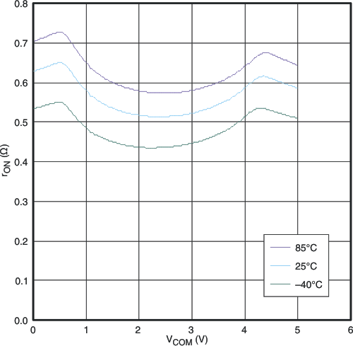
| VCC = 5 V |