SCDS285B March 2009 – August 2016 TS5A21366
PRODUCTION DATA.
- 1 Features
- 2 Applications
- 3 Description
- 4 Revision History
- 5 Pin Configuration and Functions
-
6 Specifications
- 6.1 Absolute Maximum Ratings
- 6.2 ESD Ratings
- 6.3 Recommended Operating Conditions
- 6.4 Thermal Information
- 6.5 Electrical Characteristics for 5-V Supply
- 6.6 Electrical Characteristics for 3.3-V Supply
- 6.7 Electrical Characteristics for 2.5-V Supply
- 6.8 Electrical Characteristics for 1.8-V Supply
- 6.9 Typical Characteristics
- 7 Parameter Measurement Information
- 8 Detailed Description
- 9 Application and Implementation
- 10Power Supply Recommendations
- 11Layout
- 12Device and Documentation Support
- 13Mechanical, Packaging, and Orderable Information
8 Detailed Description
8.1 Overview
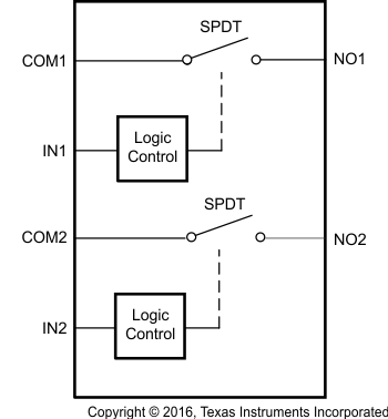
The TS5A21366 is a bidirectional, 2-channel, single-pole single-throw (SPST) analog switch that is designed to operate from 1.65-V to 5.5-V supply voltages. This device has 1.8-V compatible input control logic thresholds that are independent of the supply voltage.
8.2 Functional Block Diagram

8.3 Feature Description
8.3.1 1.8-V Compatible Control Input Threshold Independent of VCC
TS5A21366 integrates special control inputs with low threshold allowing the device to be controlled by 1.8-V signals. The thresholds are fixed and independent of the supply value (VCC). The low threshold (VIH, VIL) of the control inputs (IN1, IN2) is achieved by use of an internal bias circuit. To avoid an increased quiescent current (ICC) condition, proper power sequencing must be followed to ensure that the bias circuitry is powered up prior to applying voltage on the I/Os. The proper sequence is for the VCC pin to be brought up to VCC before the control inputs (IN1, IN2) are allowed to go to a high level.
8.3.2 Isolation in Power-Down Mode, VCC = 0
The TS5A21366 signal paths are high impedance (Hi-Z) when VCC = 0. This feature ensures the signal path is isolated when not in use to avoid interfering with other signals in the system.
8.4 Device Functional Modes
The TS5A21366 device has two functional modes. In one mode, the NO pin is connected to COM pin and a signal passes through the switch. The other mode the NO and COM pins placed in a high impedance state (Hi-Z) and a signal does not pass through the switch.
Table 2. Function Table
| IN | NO TO COM, COM TO NO |
|---|---|
| L | OFF |
| H | ON |