SCDS285B March 2009 – August 2016 TS5A21366
PRODUCTION DATA.
- 1 Features
- 2 Applications
- 3 Description
- 4 Revision History
- 5 Pin Configuration and Functions
-
6 Specifications
- 6.1 Absolute Maximum Ratings
- 6.2 ESD Ratings
- 6.3 Recommended Operating Conditions
- 6.4 Thermal Information
- 6.5 Electrical Characteristics for 5-V Supply
- 6.6 Electrical Characteristics for 3.3-V Supply
- 6.7 Electrical Characteristics for 2.5-V Supply
- 6.8 Electrical Characteristics for 1.8-V Supply
- 6.9 Typical Characteristics
- 7 Parameter Measurement Information
- 8 Detailed Description
- 9 Application and Implementation
- 10Power Supply Recommendations
- 11Layout
- 12Device and Documentation Support
- 13Mechanical, Packaging, and Orderable Information
5 Pin Configuration and Functions
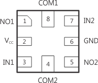
RSE Package
8-Pin UQFN
Top View

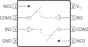
Pin Functions
| PIN | DESCRIPTION | ||
|---|---|---|---|
| NAME | VSSOP | UQFN | |
| NO1 | 1 | 1 | Switch 1, normally open |
| COM1 | 2 | 8 | Switch 1, common |
| IN2 | 3 | 7 | Switch 2, digital control pin to connect COM to NO LOW = High impedance signal path from NO pin to COM pin HIGH = NO pin connected to COM pin |
| GND | 4 | 6 | Digital ground |
| NO2 | 5 | 5 | Switch 2, normally open |
| COM2 | 6 | 4 | Switch 2, common |
| IN1 | 7 | 3 | Switch 1, digital control pin to connect COM to NO LOW = High impedance signal path from NO pin to COM pin HIGH = NO pin connected to COM pin |
| VCC | 8 | 2 | Power supply |
