ZHCSF59A October 2014 – July 2016 TS5A22364-Q1
PRODUCTION DATA.
6 Specifications
6.1 Absolute Maximum Ratings
over operating free-air temperature range (unless otherwise noted)(1) (2)| MIN | MAX | UNIT | |||
|---|---|---|---|---|---|
| VCC | Supply voltage(3) | –0.5 | 6 | V | |
| VNC | Analog voltage on NC1-NC2 pin(3) (4) (5) | VCC – 6 | VCC + 0.5 | V | |
| VNO | Analog voltage on NO1-NO2 pin(3) (4) (5) | ||||
| VCOM | Analog voltage on COM1-COM2 pin(3) (4) (5) | ||||
| II/OK | Analog port diode input clamp current | VNC, VNO, VCOM < 0 or VNC, VNO, VCOM > VCC |
–50 | 50 | mA |
| INC
INO ICOM |
On-state switch continuous current | VNC, VNO, VCOM = 0 to VCC | –150 | 150 | mA |
| On-state switch peak current(6) | –300 | 300 | |||
| IRSH | Off-state switch shunt resistor current | –20 | 20 | mA | |
| VIN | Digital input voltage | –0.5 | 6.5 | V | |
| IIK | Digital input clamp current(3) (4) | VIN < 0 | –50 | 50 | mA |
| ICC
IGND |
Continuous current through VCC or GND | –100 | 100 | mA | |
| Tstg | Storage temperature | –65 | 150 | °C | |
(1) Stresses beyond those listed under Absolute Maximum Ratings may cause permanent damage to the device. These are stress ratings only, which do not imply functional operation of the device at these or any other conditions beyond those indicated under Recommended Operating Conditions. Exposure to absolute-maximum-rated conditions for extended periods may affect device reliability.
(2) The algebraic convention, whereby the most negative value is a minimum and the most positive value is a maximum.
(3) All voltages are with respect to ground, unless otherwise specified.
(4) The input and output voltage ratings may be exceeded if the input and output clamp-current ratings are observed.
(5) This value is limited to 5.5 V maximum.
(6) Pulse at 1-ms duration <10% duty cycle.
6.2 ESD Ratings
| MIN | MAX | UNIT | ||||
|---|---|---|---|---|---|---|
| VESD | Electrostatic discharge | Human body model (HBM), per AEC Q100-002(1) | –2500 | 2500 | V | |
| Charged device model (CDM), per AEC Q100-011 | all pins | –1500 | 1500 | |||
(1) AEC Q100-002 indicates HBM stressing is done in accordance with the ANSI/ESDA/JEDEC JS-001 specification.
6.3 Recommended Operating Conditions
over operating free-air temperature range (unless otherwise noted)| MIN | MAX | UNIT | ||
|---|---|---|---|---|
| VCC | Supply voltage | 2.3 | 5.5 | V |
| VNC | Signal path voltage | VCC – 5.5 | VCC | V |
| VNO | ||||
| VCOM | ||||
| VIN | Digital control | GND | VCC | V |
6.4 Thermal Information
| THERMAL METRIC(1) (2) | TS5A22364-Q1 | UNIT | |||
|---|---|---|---|---|---|
| DGS (VSSOP) | |||||
| 10 PINS | |||||
| RθJA | Junction-to-ambient thermal resistance | 163.3 | °C/W | ||
| RθJC(top) | Junction-to-case (top) thermal resistance | 56.4 | °C/W | ||
| RθJB | Junction-to-board thermal resistance | 83.1 | °C/W | ||
| ψJT | Junction-to-top characterization parameter | 6.8 | °C/W | ||
| ψJB | Junction-to-board characterization parameter | 81.8 | °C/W | ||
| RθJC(bot) | Junction-to-case (bottom) thermal resistance | N/A | °C/W | ||
(1) For more information about traditional and new thermal metrics, see the Semiconductor and IC Package Thermal Metrics application report.
(2) The package thermal impedance is calculated in accordance with JESD 51-7.
6.5 Electrical Characteristics—2.5-V Supply
VCC = 2.3 V to 2.7 V, TA = –40°C to +125°C (unless otherwise noted) (1)| PARAMETER | TEST CONDITIONS | TA | VCC | MIN | TYP | MAX | UNIT | ||
|---|---|---|---|---|---|---|---|---|---|
| ANALOG SWITCH | |||||||||
| Analog signal | VCOM
VNO VNC |
VCC – 5.5 | VCC | V | |||||
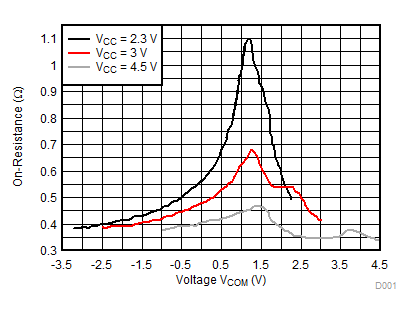
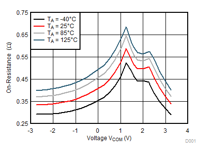
| On-state resistance |
Ron | VNC or VNO = VCC, 1.5 V, VCC – 5.5 V ICOM = –100 mA |
COM to NO or NC, See Figure 14 |
25°C | 2.7 V | 0.65 | 0.94 | Ω | |
| –40°C to +125°C | 1.3 | ||||||||
| On-state resistance match between channels |
ΔRon | VNC or VNO = 1.5 V, ICOM = –100 mA |
COM to NO or NC, See Figure 14 |
25°C | 2.7 V | 0.023 | 0.11 | Ω | |
| –40°C to +125°C | 0.15 | ||||||||
| On-state resistance flatness |
Ron(flat) | VNC or VNO = VCC, 1.5 V, VCC – 5.5 V ICOM = –100 mA |
COM to NO or NC, See Figure 14 |
25°C | 2.7 V | 0.18 | 0.46 | Ω | |
| –40°C to +125°C | 0.56 | ||||||||
| Shunt switch resistance | RSH | INO or INC = 10 mA | –40°C to +125°C | 2.7 V | 25 | 55 | Ω | ||
| On-state leakage current |
ICOM(ON) | VNC and VNO = floating, VCOM = VCC , VCC – 5.5 V |
See Figure 16 | 25°C | 2.7 V | –200 | 200 | nA | |
| –40°C to +125°C | –2500 | 2500 | |||||||
| DIGITAL CONTROL INPUTS (IN)(2) | |||||||||
| Input logic high | VIH | –40°C to +125°C | 1.4 | VCC | V | ||||
| Input logic low | VIL | –40°C to +125°C | 0.4 | V | |||||
| Input leakage current | IIH, IIL | VIN = VCC or 0 | 25°C | 2.7 V | –250 | 250 | nA | ||
| –40°C to +125°C | –250 | 250 | |||||||
| DYNAMIC | |||||||||
| Turnon time | tON | VCOM = VCC, RL = 300 Ω |
CL = 35 pF, See Figure 18 |
25°C | 2.5 V | 44 | 80 | ns | |
| –40°C to +125°C | 2.3 V to 2.7 V | 120 | |||||||
| Turnoff time | tOFF | VCOM = VCC, RL = 300 Ω |
CL = 35 pF, See Figure 18 |
25°C | 2.5 V | 22 | 70 | ns | |
| –40°C to +125°C | 2.3 V to 2.7 V | 70 | |||||||
| Break-before-make time | tBBM | See Figure 19 | 25°C | 2.5 V | 1 | 7 | ns | ||
| Charge injection | QC | VGEN = 0, RGEN = 0, |
CL = 1 nF, See Figure 23 |
25°C | 2.5 V | 215 | pC | ||
| On-State NC, NO, COM capacitance |
CCOM(ON) | VCOM = VCC or GND, Switch ON, f = 10 MHz |
See Figure 17 | 25°C | 2.5 V | 370 | pF | ||
| Digital input capacitance | CI | VIN = VCC or GND | See Figure 17 | 25°C | 2.5 V | 2.6 | pF | ||
| Bandwidth | BW | RL = 50 Ω, –3 dB | See Figure 20 | 25°C | 2.5 V | 17 | MHz | ||
| Off-state isolation | OISO | RL = 50 Ω | f = 100 kHz, See Figure 21 |
25°C | 2.5 V | –66 | dB | ||
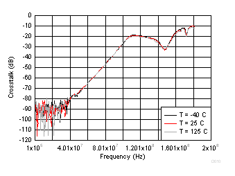
| Crosstalk | XTALK | RL = 50 Ω | f = 100 kHz, See Figure 22 |
25°C | 2.5 V | –75 | dB | ||
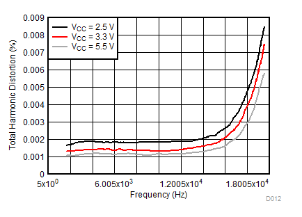
| Total harmonic distortion | THD | RL = 600 Ω, CL = 35 pF |
f = 20 Hz to 20 kHz, See Figure 24 |
25°C | 2.5 V | 0.01 | % | ||
| SUPPLY | |||||||||
| Positive supply current |
ICC | VCOM and VIN = VCC or GND, VNC and VNO = floating | 25°C | 2.7 V | 0.2 | 1.1 | μA | ||
| –40°C to +125°C | 1.3 | ||||||||
| VCOM = VCC – 5.5 V, VIN = VCC or GND, VNC and VNO = floating | –40°C to +125°C | 2.7 V | 3.3 | μA | |||||
(1) The algebraic convention, whereby the most negative value is a minimum and the most positive value is a maximum.
(2) All unused digital inputs of the device must be held at VCC or GND to ensure proper device operation. See the Implications of Slow or Floating CMOS Inputs application report, SCBA004.
6.6 Electrical Characteristics—3.3-V Supply
VCC = 3 V to 3.6 V, TA = –40°C to +125°C (unless otherwise noted) (1)| PARAMETER | TEST CONDITIONS | TA | VCC | MIN | TYP | MAX | UNIT | ||
|---|---|---|---|---|---|---|---|---|---|
| ANALOG SWITCH | |||||||||
| Analog signal | VCOM
VNO VNC |
VCC – 5.5 | VCC | V | |||||
| On-state resistance |
Ron | VNC or VNO ≤ VCC, 1.5 V, VCC – 5.5 V, ICOM = –100 mA |
COM to NO or NC, See Figure 14 |
25°C | 3 V | 0.61 | 0.87 | Ω | |
| –40°C to +125°C | 0.97 | ||||||||
| On-state resistance match between channels |
ΔRon | VNC or VNO = 1.5 V, ICOM = –100 mA |
COM to NO or NC, See Figure 14 |
25°C | 3 V | 0.024 | 0.13 | Ω | |
| –40°C to +125°C | 0.13 | ||||||||
| On-state resistance flatness |
Ron(flat) | VNC or VNO ≤ VCC, 1.5 V, VCC – 5.5 V, ICOM = –100 mA |
COM to NO or NC, See Figure 14 |
25°C | 3 V | 0.12 | 0.46 | Ω | |
| –40°C to +125°C | 0.5 | ||||||||
| Shunt switch resistance | RSH | INO or INC = 10 mA |
–40°C to +125°C | 3 V | 25 | 40 | Ω | ||
| On-state leakage current |
ICOM(ON) | VNC and VNO = floating, VCOM = VCC,VCC – 5.5 V |
COM to NO or NC, See Figure 16 |
25°C | 3.6 V | –200 | 200 | nA | |
| –40°C to +125°C | –2500 | 2500 | |||||||
| DIGITAL CONTROL INPUTS (IN)(2) | |||||||||
| Input logic high | VIH | –40°C to +125°C | 1.4 | VCC | V | ||||
| Input logic low | VIL | –40°C to +125°C | 0.6 | V | |||||
| Input leakage current | IIH, IIL | VIN = VCC or 0 | 25°C | 3.6 V | –250 | 250 | nA | ||
| –40°C to +125°C | –250 | 250 | |||||||
| DYNAMIC | |||||||||
| Turnon time | tON | VCOM = VCC, RL = 300 Ω |
CL = 35 pF, See Figure 18 |
25°C | 3.3 V | 34 | 80 | ns | |
| –40°C to +125°C | 3 V to 3.6 V | 80 | |||||||
| Turnoff time | tOFF | VCOM = VCC, RL = 300 Ω |
CL = 35 pF, See Figure 18 |
25°C | 3.3 V | 19 | 70 | ns | |
| –40°C to +125°C | 3 V to 3.6 V | 70 | |||||||
| Break-before-make time | tBBM | See Figure 19 | 25°C | 3.3 V | 1 | 7 | ns | ||
| Charge injection | QC | VGEN = 0, RGEN = 0, |
CL = 1 nF, See Figure 23 |
25°C | 3.3 V | 300 | pC | ||
| On-State NC, NO, COM capacitance |
CCOM(ON) | VCOM = VCC or GND, f = 10 MHz |
See Figure 17 | 25°C | 3.3 V | 370 | pF | ||
| Digital input capacitance | CI | VIN = VCC or GND | See Figure 17 | 25°C | 3.3 V | 2.6 | pF | ||
| Bandwidth | BW | RL = 50 Ω, –3 dB | Switch ON, See Figure 20 |
25°C | 3.3 V | 17.5 | MHz | ||
| Off-state isolation | OISO | RL = 50 Ω | f = 100 kHz, See Figure 21 |
25°C | 3.3 V | –68 | dB | ||
| Crosstalk | XTALK | RL = 50 Ω | f = 100 kHz, See Figure 22 |
25°C | 3.3 V | –76 | dB | ||
| Total harmonic distortion | THD | RL = 600 Ω, CL = 35 pF |
f = 20 Hz to 20 kHz, See Figure 24 |
25°C | 3.3 V | 0.008 | % | ||
| SUPPLY | |||||||||
| Positive supply current |
ICC | VCOM and VIN = VCC or GND, VNC and VNO = floating | 25°C | 3.6 V | 0.1 | 1.2 | μA | ||
| –40°C to +125°C | 1.3 | ||||||||
| VCOM = VCC – 5.5 V, VIN = VCC or GND, VNC and VNO = floating | –40°C to +125°C | 3.6 V | 3.4 | μA | |||||
(1) The algebraic convention, whereby the most negative value is a minimum and the most positive value is a maximum.
(2) All unused digital inputs of the device must be held at VCC or GND to ensure proper device operation. See the Implications of Slow or Floating CMOS Inputs application report, SCBA004.
6.7 Electrical Characteristics—5-V Supply(1)
VCC = 4.5 V to 5.5 V, TA = –40°C to +125°C (unless otherwise noted)| PARAMETER | TEST CONDITIONS | TA | VCC | MIN | TYP | MAX | UNIT | ||
|---|---|---|---|---|---|---|---|---|---|
| ANALOG SWITCH | |||||||||
| Analog signal | VCOM, VNO, VNC |
VCC – 5.5 | VCC | V | |||||
| On-state resistance |
Ron | VNC or VNO = VCC, 1.6 V, VCC = –5.5 V, ICOM = –100 mA |
COM to NO or NC, See Figure 14 |
25°C | 4.5 V | 0.52 | 0.74 | Ω | |
| –40°C to +125°C | 0.83 | ||||||||
| On-state resistance match between channels |
ΔRon | VNC or VNO = 1.6 V, ICOM = –100 mA |
COM to NO or NC, See Figure 14 |
25°C | 4.5 V | 0.04 | 0.23 | Ω | |
| –40°C to +125°C | 0.30 | ||||||||
| On-state resistance flatness |
Ron(flat) | VNC or VNO = VCC, 1.6 V, VCC = –5.5 V, ICOM = –100 mA |
COM to NO or NC, See Figure 14 |
25°C | 4.5 V | 0.076 | 0.46 | Ω | |
| –40°C to +125°C | 0.5 | ||||||||
| Shunt switch resistance | RSH | INO or INC = 10 mA | –40°C to +125°C | 4.5 V | 16 | 36 | Ω | ||
| On-state leakage current |
ICOM(ON) | VNC and VNO = Floating, VCOM = VCC, VCC – 5.5 V |
See Figure 16 | 25°C | 5.5 V | –200 | 200 | nA | |
| –40°C to +125°C | –2500 | 2500 | |||||||
| DIGITAL CONTROL INPUTS (IN)(2) | |||||||||
| Input logic high | VIH | –40°C to +125°C | 2.4 | VCC | V | ||||
| Input logic low | VIL | –40°C to +125°C | 0.8 | V | |||||
| Input leakage current | IIH, IIL | VIN = VCC or 0 | 25°C | 5.5 V | –250 | 250 | nA | ||
| –40°C to +125°C | –250 | 250 | |||||||
| DYNAMIC | |||||||||
| Turnon time | tON | VCOM = VCC, RL = 300 Ω |
CL = 35 pF, See Figure 18 |
25°C | 5 V | 27 | 80 | ns | |
| –40°C to +125°C | 4.5 V to 5.5 V | 80 | |||||||
| Turnoff time | tOFF | VCOM = VCC, RL = 300 Ω |
CL = 35 pF, See Figure 18 |
25°C | 5 V | 13 | 70 | ns | |
| –40°C to +125°C | 4.5 V to 5.5 V | 70 | |||||||
| Break-before-make time | tBBM | VNC = VNO = VCC/2 RL = 300 Ω |
C = 35 pF, See Figure 19 |
25°C | 5 V | 1 | 3.5 | ns | |
| Charge injection | QC | VGEN = 0, RGEN = 0 |
CL = 1L nF, See Figure 23 |
25°C | 5 V | 500 | pC | ||
| ON-State NC, NO, COM capacitance |
CCOM(ON) | VCOM = VCC or GND | See Figure 17 | 25°C | 5 V | 370 | pF | ||
| Digital input capacitance | CI | VIN = VCC or GND | See Figure 17 | 25°C | 5 V | 2.6 | pF | ||
| Bandwidth | BW | RL = 50 Ω | See Figure 20 | 25°C | 5 V | 18.3 | MHz | ||
| Off-state isolation | OISO | RL = 50 Ω | f = 100 kHz, See Figure 21 |
25°C | 5 V | –70 | dB | ||
| Crosstalk | XTALK | RL = 50 Ω | f = 100 kHz, See Figure 22 |
25°C | 5 V | –78 | dB | ||
| Total harmonic distortion | THD | RL = 600 Ω, CL = 35 pF |
f = 20 Hz to 20 kHz, See Figure 24 |
25°C | 5 V | 0.009 | % | ||
| SUPPLY | |||||||||
| Positive supply current |
ICC | VCOM and VIN = VCC or GND, VNC or VNO = floating | 25°C | 5.5 V | 0.2 | 1.3 | μA | ||
| –40°C to +125°C | 3.5 | ||||||||
| VCOM = VCC – 5.5 V, VIN = VCC or GND, VNC or VNO = floating | –40°C to +125°C | 5 | |||||||
(1) The algebraic convention, whereby the most negative value is a minimum and the most positive value is a maximum.
(2) All unused digital inputs of the device must be held at VCC or GND to ensure proper device operation. See the Implications of Slow or Floating CMOS Inputs application report, SCBA004.
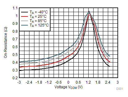
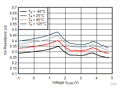
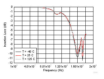
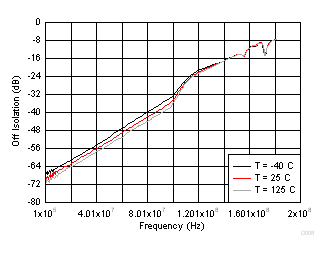
6.8 Typical Characteristics
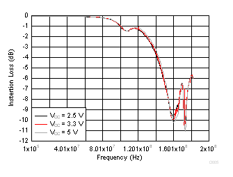

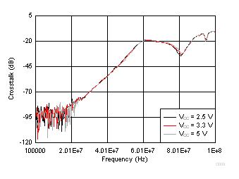


| T = 25°C | VNC and VNO = Floating | VCOM and VIN = GND |
