SCDS201H AUGUST 2005 – February 2015 TS5A23159
PRODUCTION DATA.
- 1 Features
- 2 Applications
- 3 Description
- 4 Revision History
- 5 Pin Configuration and Functions
-
6 Specifications
- 6.1 Absolute Maximum Ratings
- 6.2 ESD Ratings
- 6.3 Recommended Operating Conditions
- 6.4 Thermal Information
- 6.5 Electrical Characteristics for 5-V Supply
- 6.6 Electrical Characteristics for 3.3-V Supply
- 6.7 Electrical Characteristics for 2.5-V Supply
- 6.8 Electrical Characteristics for 1.8-V Supply
- 6.9 Typical Characteristics
- 7 Parameter Measurement Information
- 8 Detailed Description
- 9 Application and Implementation
- 10Power Supply Recommendations
- 11Layout
- 12Device and Documentation Support
- 13Mechanical, Packaging, and Orderable Information
封装选项
请参考 PDF 数据表获取器件具体的封装图。
机械数据 (封装 | 引脚)
- RSE|10
- DGS|10
散热焊盘机械数据 (封装 | 引脚)
订购信息
11 Layout
11.1 Layout Guidelines
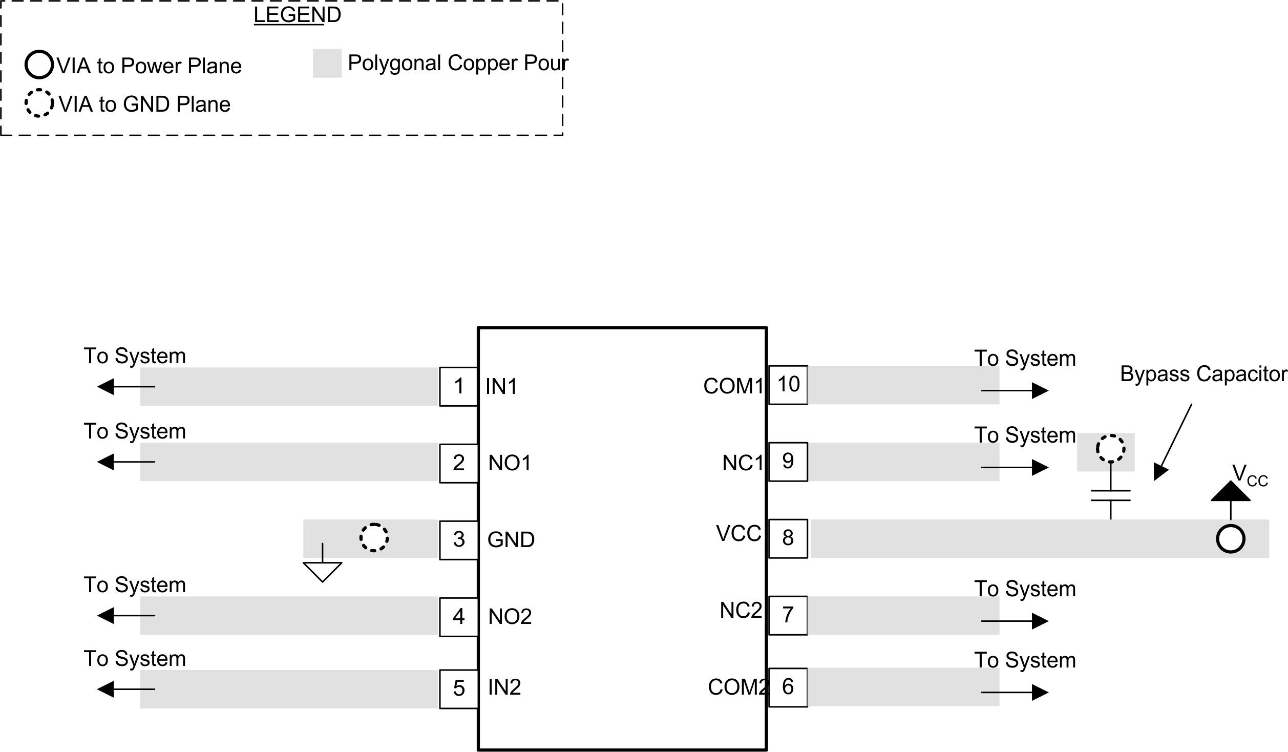
High-speed switches require proper layout and design procedures for optimum performance. Reduce stray inductance and capacitance by keeping traces short and wide. Ensure that bypass capacitors are as close to the device as possible. Use large ground planes where possible.
11.2 Layout Example
 Figure 27. Layout Recommendation