SCDS219B NOVEMBER 2005 – May 2015 TS5A3157
PRODUCTION DATA.
- 1 Features
- 2 Applications
- 3 Description
- 4 Revision History
- 5 Pin Configuration and Functions
-
6 Specifications
- 6.1 Absolute Maximum Ratings
- 6.2 ESD Ratings
- 6.3 Recommended Operating Conditions
- 6.4 Thermal Information
- 6.5 Electrical Characteristics for 5-V Supply
- 6.6 Electrical Characteristics for 3.3-V Supply
- 6.7 Electrical Characteristics for 2.5-V Supply
- 6.8 Electrical Characteristics for 1.8-V Supply
- 6.9 Typical Characteristics
- 7 Parameter Measurement Information
- 8 Detailed Description
- 9 Application and Implementation
- 10Power Supply Recommendations
- 11Layout
- 12Device and Documentation Support
- 13Mechanical, Packaging, and Orderable Information
封装选项
机械数据 (封装 | 引脚)
散热焊盘机械数据 (封装 | 引脚)
订购信息
9 Application and Implementation
NOTE
Information in the following applications sections is not part of the TI component specification, and TI does not warrant its accuracy or completeness. TI’s customers are responsible for determining suitability of components for their purposes. Customers should validate and test their design implementation to confirm system functionality.
9.1 Application Information
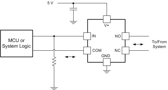
The TS5A3157 can be used in a variety of customer systems. The TS5A3157 can be used anywhere multiple analog or digital signals must be selected to pass across a single line.
9.2 Typical Application
 Figure 23. System Schematic for TS5A3157
9.2.1 Design Requirements
In this particular application, V+ was 1.8 V, although V+ is allowed to be any voltage specified in Recommended Operating Conditions. A decoupling capacitor is recommended on the V+ pin. See Power Supply Recommendations for more details.
9.2.2 Detailed Design Procedure
In this application, IN is, by default, pulled low to GND. Choose the resistor size based on the current driving strength of the GPIO, the desired power consumption, and the switching frequency (if applicable). If the GPIO is open-drain, use pullup resistors instead.
9.2.3 Application Curve
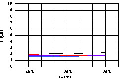
 Figure 24. Power-Supply Current vs Temperature
 (V+ = 5 V)