SCDS219B NOVEMBER 2005 – May 2015 TS5A3157
PRODUCTION DATA.
- 1 Features
- 2 Applications
- 3 Description
- 4 Revision History
- 5 Pin Configuration and Functions
-
6 Specifications
- 6.1 Absolute Maximum Ratings
- 6.2 ESD Ratings
- 6.3 Recommended Operating Conditions
- 6.4 Thermal Information
- 6.5 Electrical Characteristics for 5-V Supply
- 6.6 Electrical Characteristics for 3.3-V Supply
- 6.7 Electrical Characteristics for 2.5-V Supply
- 6.8 Electrical Characteristics for 1.8-V Supply
- 6.9 Typical Characteristics
- 7 Parameter Measurement Information
- 8 Detailed Description
- 9 Application and Implementation
- 10Power Supply Recommendations
- 11Layout
- 12Device and Documentation Support
- 13Mechanical, Packaging, and Orderable Information
封装选项
机械数据 (封装 | 引脚)
散热焊盘机械数据 (封装 | 引脚)
订购信息
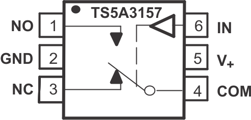
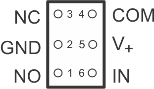
5 Pin Configuration and Functions
DBV and DCK Packages
6-Pin SOT-23 and SC-70
(Top View)

YZP Package
6-Pin DSBGA
(Bottom View)

Pin Functions
| PIN | I/O | DESCRIPTION | |
|---|---|---|---|
| NO. | NAME | ||
| 1 | NO | I/O | Normally open switch port |
| 2 | GND | — | Ground |
| 3 | NC | I/O | Normally closed switch port |
| 4 | COM | I/O | Common switch port |
| 5 | V+ | — | Power supply |
| 6 | IN | I | Switch select. High = COM connected to NO; Low = COM connected to NC. |