SCDS174D August 2004 – November 2015 TS5A3159
PRODUCTION DATA.
- 1 Features
- 2 Applications
- 3 Description
- 4 Revision History
- 5 Pin Configuration and Functions
-
6 Specifications
- 6.1 Absolute Maximum Ratings
- 6.2 ESD Ratings
- 6.3 Recommended Operating Conditions
- 6.4 Thermal Information
- 6.5 Electrical Characteristics for 5-V Supply
- 6.6 Electrical Characteristics for 3.3-V Supply
- 6.7 Electrical Characteristics for 2.5-V Supply
- 6.8 Electrical Characteristics for 1.8-V Supply
- 6.9 Switching Characteristics for 5-V Supply
- 6.10 Switching Characteristics for 3.3-V Supply
- 6.11 Switching Characteristics for 2.5-V Supply
- 6.12 Switching Characteristics for 1.8-V Supply
- 6.13 Typical Characteristics
- 7 Parameter Measurement Information
- 8 Detailed Description
- 9 Application and Implementation
- 10Power Supply Recommendations
- 11Layout
- 12Device and Documentation Support
- 13Mechanical, Packaging, and Orderable Information
7 Parameter Measurement Information
 Figure 10. ON-State Resistance (ron)
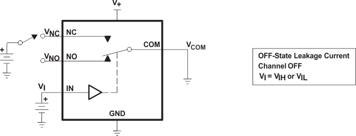
 Figure 12. ON-State Leakage Current (ICOM(ON), INC(ON), INO(ON))
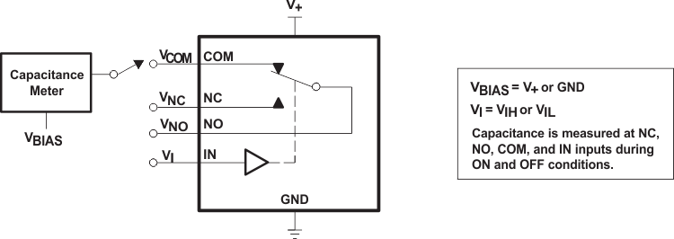
 Figure 13. Capacitance (CI, CCOM(ON), CNC(OFF), CNO(OFF), CNC(ON), CNO(ON))

1. All input pulses are supplied by generators having the following characteristics: PRR ≤ 10 MHz, ZO = 50 Ω, tr < 5 ns,
tf < 5 ns.
tf < 5 ns.
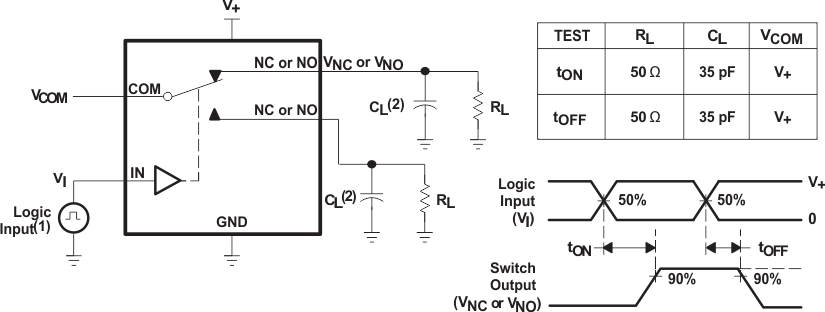
2. CL includes probe and jig capacitance.
Figure 14. Turnon (tON) and Turnoff Time (tOFF)

1. All input pulses are supplied by generators having the following characteristics: PRR ≤ 10 MHz, ZO = 50 Ω, tr < 5 ns,
tf < 5 ns.
tf < 5 ns.
2. CL includes probe and jig capacitance.
Figure 15. Break-Before-Make Time (tBBM)
 Figure 16. Bandwidth (BW)
 Figure 17. OFF Isolation (OISO)
 Figure 18. Crosstalk (XTALK)

1. All input pulses are supplied by generators having the following characteristics: PRR ≤ 10 MHz, ZO = 50 Ω, tr < 5 ns,
tf < 5 ns.
tf < 5 ns.
2. CL includes probe and jig capacitance.
Figure 19. Charge Injection (QC)

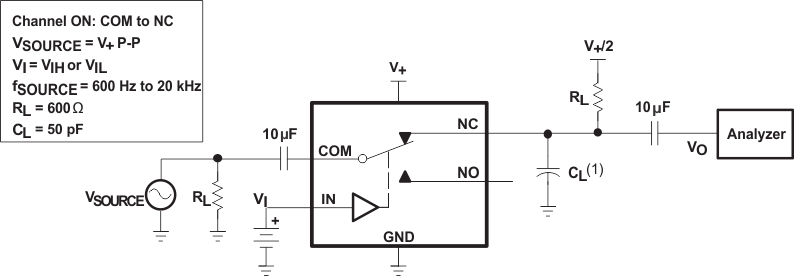
1. CL includes probe and jig capacitance.
Figure 20. Total Harmonic Distortion (THD)
