ZHCSHG2E January 2018 – April 2019 TS5MP646
PRODUCTION DATA.
8.3.1 Powered-Off Protection
When the TS5MP646 is powered off (VDD = 0 V) the I/Os and digital logic pins of the device remains in a high impedance state. The crosstalk, off-isolation, and leakage will remain within the electrical specifications. This prevents errant voltages from reaching the rest of the system and maintains isolation when the system is powering up.
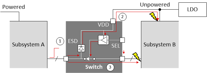
Figure 20 shows an example system containing a switch without powered-off protection with the following system level scenario.
- Subsystem A powers up and starts sending information to Subsystem B that remains unpowered.
- The I/O voltage back powers the supply rail in Subsystem B.
- The digital logic is back powered and turns on the switch. The signal is transmitted to Subsystem B before it is powered and damages it.
 Figure 20. System Without Powered-Off Protection
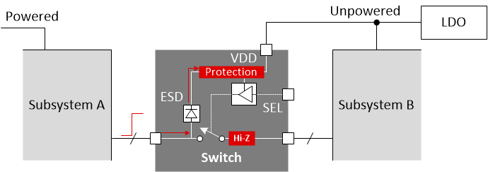
 With powered-off protection, the switch prevents back powering the supply and the switch remains high-impedance. Subsystem B remains protected.
 Figure 21. System With Powered-Off Protection
 This features has the following system level benefits.
- Protects the system from damage.
- Prevents data from being transmitted unintentionally
- Eliminates the need for power sequencing solutions reducing BOM count and cost, simplifying system design and improving reliability.