ZHCSHG2E January   2018  – April 2019 TS5MP646

PRODUCTION DATA.  

  1. 特性
  2. 应用
  3. 说明
    1.     Device Images
      1.      D-PHY 简化原理图
      2.      C-PHY 简化原理图
  4. 修订历史记录
  5. Pin Configuration and Functions
    1.     Pin Functions
  6. Specifications
    1. 6.1 Absolute Maximum Ratings
    2. 6.2 ESD Ratings
    3. 6.3 Recommended Operating Conditions
    4. 6.4 Thermal Information
    5. 6.5 Electrical Characteristics
    6. 6.6 Typical Characteristics
  7. Parameter Measurement Information
  8. Detailed Description
    1. 8.1 Overview
    2. 8.2 Functional Block Diagram
    3. 8.3 Feature Description
      1. 8.3.1 Powered-Off Protection
      2. 8.3.2 1.8-V Logic Compatible Inputs
      3. 8.3.3 Low Power Disable Mode
    4. 8.4 Device Functional Modes
      1. 8.4.1 Pin Functions
      2. 8.4.2 Low Power Disable Mode
      3. 8.4.3 Switch Enabled Mode
  9. Application and Implementation
    1. 9.1 Application Information
    2. 9.2 Typical Application
      1. 9.2.1 Design Requirements
      2. 9.2.2 Detailed Design Procedure
      3. 9.2.3 Application Curves
        1. 9.2.3.1 MIPI D-PHY Application
        2. 9.2.3.2 MIPI C-PHY Application
  10. 10Power Supply Recommendations
  11. 11Layout
    1. 11.1 Layout Guidelines
    2. 11.2 Layout Example
  12. 12器件和文档支持
    1. 12.1 文档支持
    2. 12.2 接收文档更新通知
    3. 12.3 社区资源
    4. 12.4 商标
    5. 12.5 静电放电警告
    6. 12.6 术语表
  13. 13机械、封装和可订购信息

封装选项

机械数据 (封装 | 引脚)
散热焊盘机械数据 (封装 | 引脚)
订购信息

MIPI D-PHY Application

The clock and data lanes can be interchanged as necessary to facilitate the best layout possible for the application. In addition, the signal lines of the TS5MP646 are routed single ended on the chip die. This makes the device suitable for both differential and single-ended high-speed systems. This also allows the positive and negative lines to be interchanged as necessary to facilitate the best layout possible for the application.

D-PHY application includes a differential clock and 4 differential datalanes. All the channels of the device perform similar and the clock or data signals may be interchanged as necessary to facilitate the best layout possible for the application.
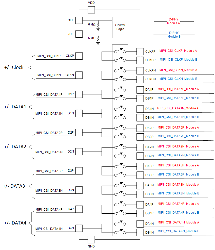
TS5MP646 DPHY_application1.gifFigure 29. MIPI D-PHY Example Pinout