SLLS413L February 2000 – June 2017 TUSB2046B , TUSB2046I
PRODUCTION DATA.
- 1 Features
- 2 Applications
- 3 Description
- 4 Revision History
- 5 Description (Continued)
- 6 Pin Configuration and Functions
- 7 Specifications
- 8 Detailed Description
- 9 Application and Implementation
- 10Power Supply Recommendations
- 11Layout
- 12Device and Documentation Support
- 13Mechanical, Packaging, and Orderable Information
7.7 Differential Driver Switching Characteristics (Low Speed Mode)
over recommended ranges of operating free-air temperature and supply voltage, CL = 50 pF (unless otherwise noted)| PARAMETER | TEST CONDITIONS | MIN | MAX | UNIT | ||
|---|---|---|---|---|---|---|
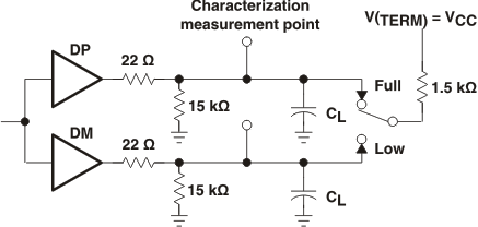
| tr | Transition rise time for DP or DM(1) | CL = 200 pF to 600 pF, | See Figure 1 and Figure 2 | 75 | 300 | ns |
| tf | Transition fall time for DP or DM(1) | CL = 200 pF to 600 pF, | See Figure 1 and Figure 2 | 75 | 300 | ns |
| t(RFM) | Rise/fall time matching(1) | (tr/tf) × 100 | 80% | 120% | ||
| VO(CRS) | Signal crossover output voltage(1) | CL = 200 pF to 600 pF | 1.3 | 2.0 | V | |
(1) Characterized only. Limits are approved by design and are not production tested.
 Figure 1. Differential Driver Switching Load
  Figure 2. Differential Driver Timing Waveforms
  Figure 3. Single-Ended Receiver Input Signal Parameter Definitions