ZHCSDS6D May   2015  – October 2017 TUSB211

PRODUCTION DATA.  

  1. 特性
  2. 应用
  3. 说明
  4. 修订历史记录
  5. Pin Configuration and Functions
  6. Specifications
    1. 6.1 Absolute Maximum Ratings
    2. 6.2 ESD Ratings
    3. 6.3 Recommended Operating Conditions
    4. 6.4 Thermal Information
    5. 6.5 Electrical Characteristics
    6. 6.6 Switching Characteristics
  7. Detailed Description
    1. 7.1 Overview
    2. 7.2 Functional Block Diagram
    3. 7.3 Device Functional Modes
      1. 7.3.1 Low Speed (LS) Mode
      2. 7.3.2 Full Speed (FS) Mode
      3. 7.3.3 High Speed (HS) Mode
      4. 7.3.4 Disable Mode
  8. Application and Implementation
    1. 8.1 Application Information
    2. 8.2 Typical Application
      1. 8.2.1 Design Requirements
      2. 8.2.2 Detailed Design Procedure
        1. 8.2.2.1 For a Host Side Application
        2. 8.2.2.2 For a Device Side Application
      3. 8.2.3 Application Curves
  9. Power Supply Recommendations
  10. 10Layout
    1. 10.1 Layout Guidelines
    2. 10.2 Layout Example
  11. 11器件和文档支持
    1. 11.1 相关链接
    2. 11.2 社区资源
    3. 11.3 商标
    4. 11.4 静电放电警告
    5. 11.5 Glossary
  12. 12机械、封装和可订购信息

封装选项

机械数据 (封装 | 引脚)
散热焊盘机械数据 (封装 | 引脚)
订购信息

Layout

Layout Guidelines

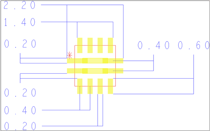
There is no need to break the USB signal trace. Thus, even with the TUSB211 powered down, or not populated, the USB link is still fully operational. To avoid the need for signal vias, routing the High Speed traces directly underneath the TUSB211 package, as illustrated in the PCB land pattern shown in Figure 8, is recommended.

Although the land pattern shown below has matched trace width to pad width, optimal impedance control is based on the user's own PCB stack-up. It is recommended to maintain 90 Ω differential routing underneath the device.

All dimensions are in millimetres (mm).

Layout Example

TUSB211 TUSB211I layout_sllseo9.gif Figure 8. DP and DM Routing Underneath Device Package