ZHCSGN1 August 2017 TUSB212-Q1
PRODUCTION DATA.
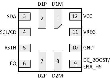
5 Pin Configuration and Functions
RWB Package
12 Pin (X2QFN)
Top View

Pin Functions
| PIN | I/O | INTERNAL PULLUP/PULLDOWN |
DESCRIPTION | |
|---|---|---|---|---|
| NAME | NO. | |||
| D1M | 1 | I/O | N/A | USB High Speed negative port.. |
| D1P | 2 | I/O | N/A | USB High Speed positive port. |
| SDA(1) | 3 | I/O | RSTN asserted: 500 kΩ PD | I2C Mode: Bidirectional I2C data pin [I2C address = 0x2C]. In non I2C mode: Reserved for TI test purpose. |
| SCL(1)/CD | 4 | I/O | RSTN asserted: 500 kΩ PD | In I2C mode: I2C clock pin [I2C address = 0x2C]. Non I2C mode: After reset: Output CD. Flag indicating that a USB device is attached (connection detected). Asserted from an unconnected state upon detection of DP or DM pull-up resistor. De-asserted upon detection of disconnect. |
| RSTN | 5 | I | 500 kΩ PU | Device disable/enable. Low – Device is at reset and in shutdown, and High – Normal operation. Recommend 0.1-µF external capacitor to GND to ensure clean power on reset if not driven. If the pin is driven, it must be held low until the supply voltage for the device reaches within specifications. |
| EQ | 6 | I | N/A | USB High Speed AC boost select via external pull down resistor. Sampled upon de-assertion of RSTN. Does not recognize real time adjustments. Auto selects max AC Boost when left floating. |
| D2P | 7 | I/O | N/A | USB High Speed positive port. |
| D2M | 8 | I/O | N/A | USB High Speed negative port. |
| DC_BOOST(2)/ENA_HS | 9 | I/O | In I2C mode: Reserved for TI test purpose. In non-I2C mode: At reset: 3-level input signal DC_BOOST. USB High Speed DC signal boost selection. H (pin is pulled high) – 80 mV M (pin is left floating) – 60 mV L (pin is pulled low) – 40 mV After reset: Output signal ENA_HS. Flag indicating that channel is in High Speed mode. Asserted upon: 1. Detection of USB-IF High Speed test fixture from an unconnected state followed by transmission of USB TEST_PACKET pattern. 2. Squelch detection following USB reset with a successful HS handshake [HS handshake is declared to be successful after single chirp J chirp K pair where each chirp is within 18 μs – 128 μs]. |
|
| GND | 10 | P | N/A | Ground |
| VREG | 11 | O | N/A | 1.8-V LDO output. Only enabled when operating in High Speed mode. Requires 0.1-µF external capacitor to GND to stabilize the core. |
| VCC | 12 | P | N/A | Supply power |
(1) Pull-up resistors for SDA and SCL pins in I2C mode should be 2 kΩ (5%). If both SDA and SCL are pulled up at reset the device enters into I2C mode.
(2) Pull-down and pull-up (to 3.3 V) resistors for DC_BOOST pins must be between 22 kΩ to 47 kΩ in non I2C mode.