ZHCSGQ5 September   2017 TUSB215-Q1

PRODUCTION DATA.  

  1. 特性
  2. 应用
  3. 说明
  4. 修订历史记录
  5. Pin Configuration and Functions
  6. Specifications
    1. 6.1 Absolute Maximum Ratings
    2. 6.2 ESD Ratings
    3. 6.3 Recommended Operating Conditions
    4. 6.4 Thermal Information
    5. 6.5 Electrical Characteristics
    6. 6.6 Switching Characteristics
    7. 6.7 Typical Characteristics
  7. Detailed Description
    1. 7.1 Overview
    2. 7.2 Functional Block Diagram
    3. 7.3 Feature Description
      1. 7.3.1 EQ
      2. 7.3.2 DC BOOST
      3. 7.3.3 BC1.2 CDP Support
    4. 7.4 Device Functional Modes
      1. 7.4.1 Low Speed (LS) Mode
      2. 7.4.2 Full Speed (FS) Mode
      3. 7.4.3 High Speed (HS) Mode
      4. 7.4.4 Shutdown Mode
      5. 7.4.5 I2C Mode
  8. Application and Implementation
    1. 8.1 Application Information
    2. 8.2 Typical Application
      1. 8.2.1 Design Requirements
      2. 8.2.2 Detailed Design Procedure
        1. 8.2.2.1 Test Procedure to Construct USB High Speed Eye Diagram
          1. 8.2.2.1.1 For a Host Side Application
          2. 8.2.2.1.2 For a Device Side Application
      3. 8.2.3 Application Curves
  9. Power Supply Recommendations
  10. 10Layout
    1. 10.1 Layout Guidelines
    2. 10.2 Layout Example
  11. 11器件和文档支持
    1. 11.1 接收文档更新通知
    2. 11.2 社区资源
    3. 11.3 商标
    4. 11.4 静电放电警告
    5. 11.5 Glossary
  12. 12机械、封装和可订购信息

封装选项

请参考 PDF 数据表获取器件具体的封装图。

机械数据 (封装 | 引脚)
  • RGY|14
散热焊盘机械数据 (封装 | 引脚)
订购信息

Layout

Layout Guidelines

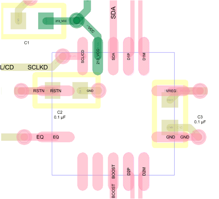
To avoid the need for signal vias, it is highly recommend to route the High Speed traces on the same surface layer than the TUSB215-Q1 is placed. shows an example how one could layout the PCB for TUSB215-Q1.

The layout should use impedance controlled traces to maintain 90 Ω differential impedance for the whole signal path as required per USB 2.0 specification. General guidelines for highspeed signal routing apply.

Layout Example

TUSB215-Q1 layoutsnippet.gif Figure 22. Layout Example