ZHCSIS9A September   2018  – December 2018 TUSB217-Q1

PRODUCTION DATA.  

  1. 特性
  2. 应用
  3. 说明
    1.     Device Images
      1.      简化原理图
  4. 修订历史记录
  5. Pin Configuration and Functions
    1.     Pin Functions
  6. Specifications
    1. 6.1 Absolute Maximum Ratings
    2. 6.2 ESD Ratings
    3. 6.3 Recommended Operating Conditions
    4. 6.4 Thermal Information
    5. 6.5 Electrical Characteristics
    6. 6.6 Switching Characteristics
    7. 6.7 Timing Requirements
  7. Detailed Description
    1. 7.1 Overview
    2. 7.2 Functional Block Diagram
      1. 7.2.1 Functional Block Diagram
    3. 7.3 Feature Description
      1. 7.3.1 High speed boost
      2. 7.3.2 RX Sensitivity
    4. 7.4 Device Functional Modes
      1. 7.4.1 Low Speed (LS) mode
      2. 7.4.2 Full Speed (FS) mode
      3. 7.4.3 High Speed (HS) mode
      4. 7.4.4 High Speed downstream port electrical compliance test mode
      5. 7.4.5 Shutdown mode
      6. 7.4.6 I2C mode
    5. 7.5 TUSB217 Registers
      1. 7.5.1 EDGE_BOOST Register (Offset = 0x1) [reset = X]
        1. Table 4. EDGE_BOOST Register Field Descriptions
      2. 7.5.2 CONFIGURATION Register (Offset = 0x3) [reset = X]
        1. Table 5. CONFIGURATION Register Field Descriptions
      3. 7.5.3 DC_BOOST Register (Offset = 0xE) [reset = X]
        1. Table 6. DC_BOOST Register Field Descriptions
      4. 7.5.4 RX_SEN Register (Offset = 0x25) [reset = X]
        1. Table 7. RX_SEN Register Field Descriptions
  8. Application and Implementation
    1. 8.1 Application Information
    2. 8.2 Typical Application
      1. 8.2.1 Design Requirements
      2. 8.2.2 Detailed Design Procedure
        1. 8.2.2.1 Test Procedure to Construct USB High Speed Eye Diagram
          1. 8.2.2.1.1 For a Host Side Application
          2. 8.2.2.1.2 For a Device Side Application
      3. 8.2.3 Application Curves
  9. Power Supply Recommendations
  10. 10Layout
    1. 10.1 Layout Guidelines
    2. 10.2 Layout Example
  11. 11器件和文档支持
    1. 11.1 文档支持
    2. 11.2 接收文档更新通知
    3. 11.3 社区资源
    4. 11.4 商标
    5. 11.5 静电放电警告
    6. 11.6 术语表
  12. 12机械、封装和可订购信息

封装选项

请参考 PDF 数据表获取器件具体的封装图。

机械数据 (封装 | 引脚)
  • RGY|14
散热焊盘机械数据 (封装 | 引脚)
订购信息

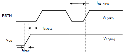
Timing Requirements

MIN NOM MAX UNIT
POWER UP TIMING
TRSTN_PW Minimum width to detect a valid RSTN signal assert when the pin is actively driven low 100 µs
TSTABLE VCC must be stable before RSTN de-assertion 300 µs
TREADY Maximum time needed for the device to be ready after RSTN is de-asserted. 500 µs
TRAMP VCC ramp time 0.2 100 ms
I2C (STD)
tSUSTO Stop setup time, SCL (Tr=600ns-1000ns), SDA (Tf=6.5ns-106.5ns), 100kHz STD  4     µs
tHDSTA Start hold time, SCL (Tr=600ns-1000ns), SDA (Tf=6.5ns-106.5ns), 100kHz STD 4     µs
tSUSTA Start setup time, SCL (Tr=600ns-1000ns), SDA (Tf=6.5ns-106.5ns), 100kHz STD 4.7 µs
tSUDAT Data input or False start/stop, setup time, SCL (Tr=600ns-1000ns), SDA (Tf=6.5ns-106.5ns), 100kHz STD 250 ns
tHDDAT Data input or False start/stop, hold time, SCL (Tr=600ns-1000ns), SDA (Tf=6.5ns-106.5ns), 100kHz STD 5 µs
tBUF Bus free time between START and STOP conditions 4.7 µs
tLOW Low period of the I2C clock 4.7 µs
tHIGH High period of the I2C clock 4 µs
tF Fall time of both SDA and SCL signals 300 ns
tR Rise time of both SDA and SCL signals 1000 ns
TUSB217-Q1 RESET-DIAG.gifFigure 1. Power On and Reset Timing
TUSB217-Q1 I2C-TIMING.gifFigure 2. I2C Timing